
Full Wave Matching Circuit Optimization in XFdtd®

Determining the final set of component values in a matching network can be a challenging process. Traditionally, RF engineers have had to simplify and idealize their matching circuits in schematics that are separated from the EM simulation. This simplification into a lumped element schematic requires perfect grounds and leaves out the coupling and transmission line effects of the interconnect metal and the antennas.
Now design engineers can optimize matching circuit lumped element values directly in the EM layout where the coupling from multiple antennas and the ground return current paths are taken into account, using XFdtd’s Circuit Element Optimizer.
XFdtd’s Circuit Element Optimizer Simplifies and Speeds the Process of Matching the Antenna
XF’s Circuit Element Optimizer determines lumped element component values based on the following goals:
- Radiation efficiency
- System efficiency
- S-parameters
The Circuit Element Optimizer and matching circuit elements remain in the EM layout structure, simplifying the antenna matching work flow.
Recent and upcoming technologies in mobile 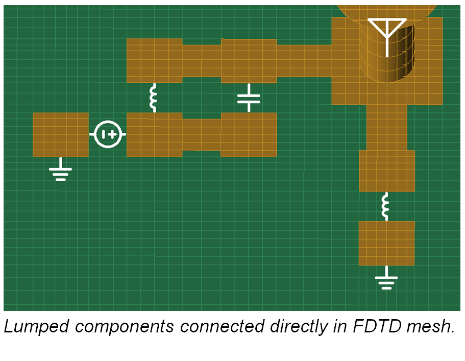 applications, such as inter-band carrier aggregation and new frequency bands, present difficult challenges for antenna designers. Several antennas, each serving multiple bands, may interact with both the device and one another, affecting the antenna match simultaneously. Optimizing in the EM space, the Circuit Element Optimizer addresses these problems. The ability to design devices for multiple mobile carriers is also simplified with support for tunable components, while trade-offs in efficiencies between different scenarios (free space, head and hand, etc.) are realized with the optimizer’s support for different physical configurations.
In addition to inter-band carrier aggregation, the Circuit Element Optimizer can also be used for general antenna matching circuit applications, including:
- Matching circuits for single antenna with single band of operation
- Matching circuits for single antennas with multiple bands (with or without tunable components)
- Matching circuits for multiple antennas including MIMO