What Technology Developments Are Needed For Millimeter-Wave 5G?
By Liam Devlin, Plextek RFI
5G is intended to offer a step change in data rates, with seemingly infinite capacity. The availability of new mm-Wave frequency bands, where large contiguous bands of spectrum can be exploited, is key to achieving these ambitious mobile data rate targets.
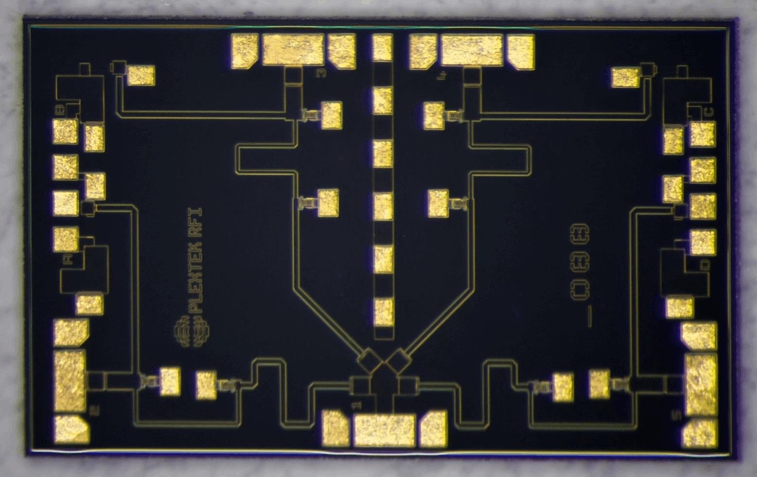
Although the 5G mm-Wave frequency allocations will not be finalized until 2019, much development work already is under way, in a number of different candidate bands, and numerous demonstrator systems are being designed, assembled, and trialed. For example, Plextek RFI already is developing mm-Wave front ends for deployment in some of the first high-frequency 5G demonstrator systems. These component designs include power amplifiers (PA), switches, low-noise amplifiers (LNA), phase shifters, and multifunction MMICs. All of this 5G work is taking place in GaAs pHEMT technology, with the exception of some of the high-linearity mm-Wave switches, which use an integrated PIN diode process.
5G Challenges
There are several challenges to working at these higher frequencies. The capabilities of the GaAs technology begin to decline, so it is crucial to extract the very best performance from a design. Careful design of packaging to minimize parasitics is a priority that must be considered from the outset. Fewer processes are available to offer the required performance at the higher frequencies, and the use of accurate EM simulation also becomes more essential.
There is a considerable amount of commonality between the specifications for components to be used in base stations and those intended for user terminals. This is because, for 5G, the base station size will be small and the density of base stations will be high. Much more emphasis will be placed on transmitting the data back to an optical trunk network, as quickly as possible, because of the huge amounts of traffic involved.
The functionality and performance targets for 5G are ambitious: Data rates in excess of 10 GB/s, extremely low latency, and uniform coverage over a wide area, as well as a thousand-fold increase in capacity are the main aims. 5G also is expected to enable and encourage the development of new markets, technologies, and applications beyond high-speed mobile communications — including massive machine-type communications (mMTC), mission-critical applications (like autonomous vehicles), and even last-mile fixed broadband.
Historically, the mm-Wave bands above 24GHz were considered inappropriate for mobile and non-line-of-sight use. However, recent research has shown that the issues can be addressed and overcome, and utilizing these bands — alongside new and existing sub-6GHz bands — will be a key factor in the new 5G radio interface. In advance of the specific frequency bands being finalized, we have been able to form a picture of the bands where most current design activity is taking place, based on the work Plextek RFI is performing for its clients and inquiries the company receives.
The likely operating frequencies include the nominal 28 GHz (27.5 - 28.35GHz), 37 GHz (37 - 38.6GHz) and 39 GHz (38.6 - 40GHz) bands, all of which already are licensed by the FCC. In Europe, the Radio Spectrum Policy Group (RSPG) has recommended the 26 GHz band (24.25 to 27.5GHz); this is being promoted as the “Pioneer Band” for 5G in Europe, as well as the priority band for global harmonization. Bands around 32 GHz and 42 GHz also have been highlighted as longer-term options.
We see 28 GHz and 39 GHz as the bands where the first commercial products are likely to emerge. Following that, the 26 GHz Pioneer Band may start to become important. As with previous generations, it is unlikely that a single global spectrum allocation will emerge, so there will be distinct benefits in having at least dual-band components available. We can predict that there will ultimately be a need for tri-band and even quad-band components, which will present a real challenge for designers.
Technology Choices
Most mm-Wave 5G systems will be based on some form of beam steering, such as phased-array or switched beam antennas, and Plextek RFI already has been involved in designing custom MMICs for such prototype systems. GaAs pHEMT processes are considered an attractive option for PAs in particular, as they offer adequate RF power output, high linearity, and high power-added efficiency (PAE) at a modest supply voltage. GaN, which is growing in popularity for many applications, is another contender that offers higher power density, but has the disadvantage of requiring a higher supply voltage.
GaAs pHEMT also is a good option for LNAs due to its superior noise figure performance. In the longer term, the LNA may be integrated into a transceiver, and then SiGe — or even CMOS or silicon-on-insulator (SOI) — would be the likely technology choice. For upconverters and downconverters, Plextek RFI is working on pHEMT solutions, but we know of other companies using SiGe, CMOS, and SOI.

mm-Wave Packaging Options
The packaging of mm-Wave ICs can present some significant challenges, since at these high frequencies, even short bond wires have appreciable inductive parasitics. Additionally, the parasitics of the package and the PCB on which it is to be mounted must be considered if optimum performance is to be obtained for the packaged part. With careful design and attention to detail, there are several SMT packaging options that can be used to provide good performance at mm-Wave.
Overmolded plastic packages, where the device is assembled onto a leadframe and covered with a plastic compound, typically are usable up to about 30 - 40 GHz, depending on the functionality of the IC. We have successfully used air-cavity plastic packages — similar to overmolded but with an air-filled cavity above the device — up to 42 GHz. In both of these cases, a custom leadframe often is required to optimize performance. For higher frequencies, laminate packages can be custom-designed: these allow the chip surface to sit at the same level as the package, therefore permitting the use of shorter bond wires, and can work up to about 45 GHz. We designed a custom laminate package for a third-party 39 GHz switch IC for 5G that already has shipped several thousand units, even before the 5G standards have been defined.
Multi-Band Components

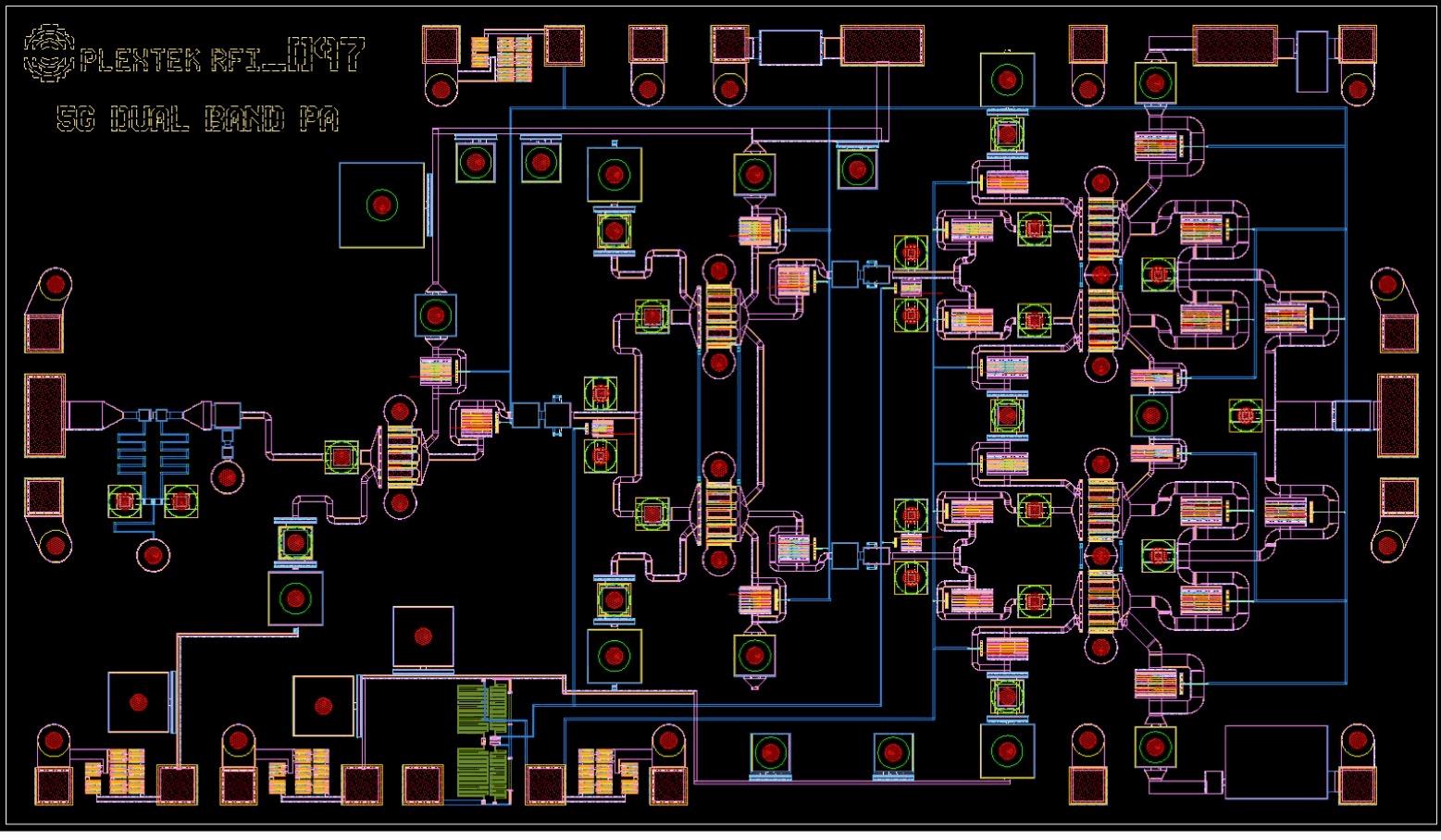
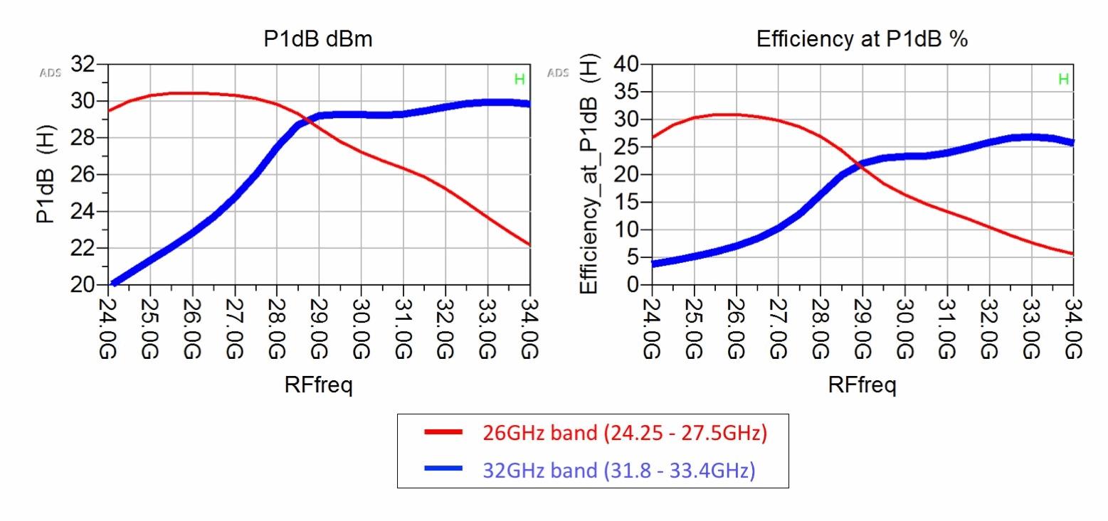
However, at these frequencies, FETs act more as variable reactances than as conventional switches transitioning between a high and a low impedance. The chip achieved a power output of approximately 1W in each of the bands, and a PAE of 27 – 30 percent, as shown in Fig. 3. There is some trade-off in PAE for the dual-band design, but cost-effectiveness is a major consideration for components to be used in mobile devices, and the figures being achieved still are acceptable.

Conclusion
Innovation in mm-Wave chip and component design for 5G is taking place very rapidly, owing to the massive resources being dedicated to it. Here, we have described the latest trends and some recent results in both device and packaging technology, including demonstrating the achievability of the dual-band components that will be required for high-volume 5G terminals, due to the number of different mm-Wave spectrum allocations likely to be made available around the world.
About The Author
Liam Devlin is the CEO of Plextek RFI, a UK-based design house specialising in the design and development of RFICs, MMICs and microwave/mm-wave modules. He has led the design and development of over 90 custom ICs on a range of GaAs, GaN and Si processes at frequencies from baseband to 90GHz, and has also developed microwave and mm-wave sub-systems using a variety of technologies. Prior to joining Plextek he was Chief Designer with Marconi Caswell, where he designed GaAs ICs for both the commercial product line and for customer specific applications, and was formerly employed by Philips Research Laboratories. Liam has a B.Eng in Electrical and Electronic Engineering from the University of Leeds, and has published over 50 technical papers.
