
Vector Modulation Techniques for Digital RF Systems—Part Two
By: Frank Zavosh, Mike Thomas, David Ngo, Tracy Hall, ON Semiconductor (Semiconductor Components Industries LLC)
Contents
Bandwidth efficiency limits
Digital filters
Common pre-modulation filters
Gaussian filter
Test system setup
Wrap Up
This is the second part in a two-part set on vector communication schemes for wireless communications systems. In part one, we discussed the key digital modulation techniques used in modern wireless designs In this part, we will explore efficiency, digital filtering, and system set up for the measurement of spectral and time domain analysis.
Bandwidth efficiency limits
One of the most significant characteristics of a vector modulation scheme is the bandwidth it uses to transmit a given set of data. This is best quantified in terms of bandwidth efficiency limit.
Bandwidth efficiency describes how the allocated bandwidth is utilized by the modulation scheme to transmit data. The most common representation of bandwidth efficiency in digital modulation is given by the equation:
Spectral Efficiency [b/s/Hz] = 1/(2*(f-fc)Tb)
Note the factor 2 is present because we are dealing with double sideband quadrature modulated systems.
The theoretical bandwidth efficiency limits for a number of modulation types are given in Table 1.
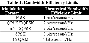
The Power levels are normalized in this case. Note that these figures cannot actually be achieved in practical systems since they require perfect modulators, demodulators, filters and transmission paths. In general, the baud rate required, bandwidth availability, and the sensitivity of the receiver used will dictate which of the modulation formats can used of a given system. Digital filters further enhance bandwidth efficiency.
Digital filters
Any fast transition in a signal, whether it is amplitude, phase, or frequency, will require a wide occupied bandwidth. Any technique that helps to slow down these transitions will narrow the occupied bandwidth. Digital filtering serves to smooth these transitions, thus, enhancing the spectral efficiency of modulated signals. In addition, on the receive end, reduced bandwidth due to filtering improves sensitivity since more noise and interference are rejected.
The spectral efficiency of filtered signals is achieved at a cost of increased system complexity and size, potential increase in power requirements in data transmission, and increased intersymbol interference (ISI). Clearly the addition of a high-order digital filters will require substantial increase in number of devices required in the circuit. The increase in power requirement is due to the overshoots in the signal trajectories, which represents carrier power and phase. The ISI occurs when the signal is filtered enough so that the symbols blur together and each symbol affects those around it. Therefore, some tradeoffs must be made whenever filters are used to shape the baseband waveforms carrying digital information.
One straightforward approach to the design of digital filters is to window or truncate the ideal prototype response. However, direct truncation (i.e. rectangular windowing) leads to the well-known Gibbs phenomenon, which manifests itself as a large ripple in the frequency response of the filter in the vicinity of the filter magnitude discontinuities (i.e. near edges of the pass and stopbands). Furthermore, this ripple amplitude does not decrease with increasing filter duration.
Hence, direct truncation, or rectangular windowing, is rarely used in practice. A more successful way of windowing is by gradually tapering the amplitude to zero near the ends of the filter with a weighting sequence, known as a window. The resulting filter response is then the product of the window and the ideal filter response.
The windows initially used in finite impulse response (FIR) digital filter design included Hamming, Hanning, Blackman, and Boxcar. These windows always produce fixed ripple in both passband and stopband. However, another class of FIR filters have been developed which use a set of variable parameters to control the ripple, both in the passband and stopband. These filters are more commonly used in digital communications today.
Common pre-modulation filters
The most common pre-modulation filters used in digital communications systems include raised cosine, square-root raised cosine, and Gaussian filters. A general block diagram of one of these filters is shown in Figure 5. Note that only three operations, namely time delays (at symbol time), multiplications, and summations, are used in their design. This is generally implemented in an application-specific IC (ASIC) hardware (for speed) or in software using a multi-purpose digital signal processor (DSP).

Raised cosine filters have the property that their impulse response rings at the symbol rate. The filter is chosen to ring, or have the impulse response of the filter cross through zero, at the symbol clock frequency. As a result the adjacent symbols do not interfere with each other at the symbol times because the response equals zero at all symbol times except the center (desired) one.
Usually, the filter is split—half in the transmitter path and half in the receiver path. In this case, root Nyquist filters are used in each part. The impulse response of a root Nyquist filter is given below.
h(t) = [sin(pt/Ts)/ (pt/Ts)]. [cos(pat/Ts)/(1-4(at/Ts)2]
Note that the frequency response of the filter is modified by varying the parameter *, and the final value of t, which is defined in terms of the number of zero crossing (taps).
Gaussian filter
In contrast to the raised cosine filter, the Gaussian filter does not have zero ISI. Gaussian filters are used because of their advantages in carrier power, occupied bandwidth, and symbol-clock recovery. These filters are Gaussian shape in both the time and frequency domains. This shape effects in the time domain are relatively short and each symbol interacts significantly with only the preceding and succeeding symbols. The transfer functions is represented as:
h(t) = [(BTs) * (2p/ln(2))1/2]. exp[-2(ptBTs) 2/ln(2)]
The frequency response of a Gaussian filter is determined by the final value of t and the parameter BTs. However, the sensitivity to the final value of t is significantly less than that of the raised cosine filter due to the rapid decaying nature of the Gaussian Function.
Test system setup
In order to analyze the performance of RF circuits designed for digital communications systems, either an arbitrary waveform generator (AWG) or a software package is commonly used to generate the baseband signals representing the input data. These signals are then mixed with the RF carrier either internally in the AWG or externally and injected into the RF circuit. This allows the designer to evaluate the performance of designs without expending a great deal of time and energy on the IF and baseband portions of the system. A similar approach is also used in analyzing received signals once they have been downconverted.
There are two drawbacks to the above approach. First, the hardware/software required in such a setup tend to be expensive. Second, the range of baseband signals that can be considered are limited to those provided by the hardware or software package. This means that not all combinations of source and channel encoding, modulations, and filtering can be considered.
Furthermore, the designer is not able to generate none standard baseband signals for analysis. The need for such signal can arise for example, when a specific baseband signal is required in studying a digital pre-distortion scheme for power amplifier linearization or a software-defined radio (SDR).
To alleviate the aforementioned problems, a fully software-based baseband signal generator can be developed with interfaces to the hardware via a GPIB card (Figure 6).
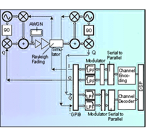
Figure 6 depicts a system where the baseband signals are synthesized for transmit components and are processed and analyzed from the receive components. In addition, other baseband signals can potentially be injected at intermediate stages such as the AWGN and Rayleigh fading sources illustrated in the figure. The hardware portion of the system consists of upconverter, power amplifier (PA), and downconverter blocks, including carrier recovery and analog filters.
For the purpose of extracting and analyzing data at the various stages in the system, a test bench is used (Figure 7). The test bench encompasses a standard PC with a GPIB controller card used for interfacing with the bench equipment, consisting of a dual-channel AWG, a digital sampling scope, a spectrum analyzer, an RF signal generator, a quadrature phase splitter, a phase shifter, a resistive combiner, and a direct quadrature modulator.
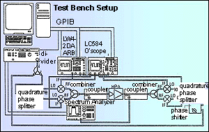
In the test bench setup, the phase shifter is used to equalize the delay in the local oscillator (LO) path allowing proper quadrature demodulation of the baseband signals. The spectrum analyzer, on the other hand, is employed to study the frequency response of baseband and modulated carriers. Specifically, the spectrum analyzer allows engineers to study the frequency characteristics of various digital filters as well as the spectral efficiency of various modulation schemes.
As stated above, a digital sampling scope is also employed in the test bench setup. This scope is used to study the eye diagram, constellation, phase trellis, and I/Q waveforms of the various quadrature modulations. These graphical representations of the generated baseband signals shed light on bit-error rate (BER), spectral efficiency, circuit non-linearity, and power efficiency of modulations considered.
Through the test bench, engineers can extract and examine data at various stages in the system. By doing this, engineers can better determine the performance capabilities of their system. In addition, they can quickly identify problems where they occur during the transmit and/or receive process.
Wrap up
As wireless systems become more sophisticated, the need for complex modulation schemes will continue to grow. By properly understanding these schemes, RF designers can ease the design process and better develop components and systems.
References
1. V.J. Garg, J.E. Wilkes, Wireless And Personal Communications Systems, Prentice Hall, 1996.
2. Hewlett-Packard, "Digital Modulation in Communications Systems-An Introduction," Application Note 1298, 1997.
3. J.D. Oetting, "A Comparison of Modulation Techniques for Digital Radio," IEEE Trans. On Comms., Dec. 1979, pp. 1752-1762.
4. D. Hanselman, B. Littlefield, Matlab The Language Of Technical Computing, Prentice Hall, 1997.
5. P. Marchand, Graphics And GUIs With Matlab, CRC Press, 1996.
6. K. Feher, Wireless Digital Communications, Prentice Hall, 1995.
7. K. Feher, H. Mehdi, "Modulation/Microwave Integrated Digital Wireless Developments," IEEE Trans .On Microwave Theory and Tech., Jul. 1995, pp. 1715-1731.
8. Y. Imai, "Telecommunications Moves Toward Digital Standards," Microwave & RF., Dec. 1995, pp. 95-100.
9. N. Boutin, "Complex Signals: Part 1," RF Design, Dec. 1989, pp. 27-32.
10. N. Boutin, "Complex Signals: Part II," RF Design, Jan. 1990, pp. 57-65.
11. T. Noguchi, Y. Daido, J.A. Nossek, "Modulation Techniques for Microwave Digital Radio," IEEE comms. Magazine, Oct. 1986, pp. 21-30.
12. M. Kettrick, "Digital Modulation Basics," Anritsu Presentation, pp. 1-22.
13. S.A. Gronemeyer, A.L. McBride, "MSK And Offset QPSK Modulation," IEEE Trans. On Communications, Aug. 1976, pp. 809-819.
14. A.H. Higashi, "Digital Modulation Overview," Motorola SPS Presentation,, Jun. 1998, pp. 1- 34.
15. R. Umstattd, "Assay Quadrature Modulators For PCS Applications," Microwave & RF, Aug. 1993, pp. 90-102.
16. S. Pasupathy, "Minimum Shift Keying: A Spectrally Efficient Modulation," IEEE Communications Magazine, Jul. 1979, pp. 14-22.
17. R.E. Ziemer, C.R. Ryan, J.H. Stilwell, "Conversion and Matched Filter Approximation for Serial Minimum-Shift Keyed Modulation," IEEE Trans. On Communications, Mar. 1982, pp. 495-509.
18. F. Amoroso, J.A. Kivett, "Simplified MSK Signaling Technique," IEEE Trans. On Communications, Apr. 1977, pp. 433-441.
19. J.W. Bayless, R.D. Pedersen, "Efficient Pulse Shaping Using MSK Or PSK Modulation," IEEE Trans. On Communications, Jun. 1979, pp. 927-930.
20. M. Rabzel, S. Pasupathy, "Spectral Shaping In Minimum Shift Keying (MSK)-Type Signals," IEEE Trans. On Communications, Jan. 1978, pp. 189-195.
21. D.H. Morais, K. Feher, "The Effect Of Filtering And Limiting On The Performance Of QPSK, Offset QPSK, And MSK Systems," IEEE Trans. On Communications, Dec. 1980, pp. 1999-2009.
22. K. Murota, K. Hirade, "GMSK Modulation For Digital Mobile Radio Telephony," IEEE Trans. On Communications, Jul. 1981, pp. 1044-1050.
23. A.L. Linz, A. Hendrickson, "Efficient Implementation of an I-Q GMSK Modulator," IEEE Trans. On Circuits and Systems, Jan. 1996, pp. 14-23.
24. J. Lee, . Liu, H. Samueli, "A Digital Adaptive Beamforming QAM Demodulator IC for High Bit-Rate Wireless Communications," IEEE Journal Of Solid-State Circuits, Mar. 1998, pp. 367-376.
25. C.S. Koukourlis, "Hardware Implementation Of A Differential QAM Modem," IEEE Trans. On Broadcasting., Sep. 1997, pp. 281-287.
26. A. Lymer, "Digital-Modulation Scheme Processes RF Broadcast Signals," Microwave & RF, Apr. 1994, pp. 149-159.
27. N. Boutin, "Complex Signals: Part IV," RF Design, May 1990, pp. 65-75.
28. K.M. Prabhu, K.B. Bagan, "FIR Digital Filter Design with Variable Parameter window Families," Journal of the Institution of Electrical and Radio Engineers, Dev. 1988, pp. 295-298.
29.
A.N. D'Andrea, F. Guglielmi, U. Mengali, A. Spalvieri, "Design Of Transmit And Receive Digital Filters For Data Communications," IEEE Trans. On Communications, Feb./Mar./Apr. 1994, pp. 357-359.
30. J.H. McClellan, R.W. Schafer, M.A. Yoder, DSP First A Multimedia Approach, Prentice Hall, 1998.
About the authors:
Frank Zavosh, RF Design Engineer; Mike Thomas, RF Design Engineer; David Ngo, RF Design Engineer; and Tracy Hall, RF Design Engineer, Motorola Semiconductor Product Sector, 210 East Elliot Road, Phoenix, AZ, 85284. 480-413-6617; Fax: 480-413-4433.