
Understanding Diamond As A Material For RF Packaging
By Firooz N. Faili, Element Six

Diamond is one of the most sought-after materials in the world, most commonly as a luxurious personal good. However, diamond’s remarkable material properties make it an ideal engineering material. With extreme performance in the most challenging conditions, its unique mechanical, optical, thermal, and electrochemical properties make it effective for a range of industrial uses.
The secret to diamond’s incredible hardness lies in the structure: tetrahedral covalent bonds between its four nearest neighbors, linked in a cubic lattice. This strongly bonded, tightly packed, dense, and rigid structure gives rise to many of diamond’s properties.
Natural Or Synthetic?
All diamonds, whether synthetic or natural, are made of the same material and display the same chemical structure and physical properties. However, synthetic diamonds offer control over defects and synthesis conditions, giving manufacturers the ability to optimize and tailor their properties for a wide range of applications.
What Can Diamond Be Used For?
While most people think of natural diamond as aesthetically unique and the pinnacle of hardness, its synthetic counterpart delivers benefits for a range of industries. Its hardness makes it an ideal material for automotive and aerospace cutting tools, particularly with composites that are typically difficult to machine.
Optical quality diamond delivers outstanding benefits to high-power laser applications. No other material can contest diamond’s combination of broadband transparency, low absorption, and excellent thermal conductivity. In multi-kW and high-power density applications, these properties allow diamond optics to last significantly longer, and with less thermal distortions, than alternative materials.
Diamond electrodes can be used for the treatment of industrial wastewater and landfill leachates, which are difficult to treat by conventional means. The production of ozone by electrolysis can be made more efficient and economical with the use of long-lasting diamond electrodes.
Diamond also has the potential to transform electrochemical sensing. All the unique and engineered properties of synthetic diamond — high thermal conductivity, light transmission, inertness, and radiation hardness — can contribute to greatly enhanced performance in this field.
In high-frequency electronics applications, diamond’s utility is evident in the cooling of high-power density hot spots, as well as maintaining low VSWR as high-frequency resistive termination, limiters, and attenuators, and as high-frequency filters or resonators in surface acoustic wave (SAW) devices.
Two Production Methods
The vast majority of synthetic diamond is made by high pressure and high temperature (HPHT) methods, replicating the natural conditions in which diamond forms. The materials form in large presses, weighing hundreds of tons, to produce pressure equivalent to an inverted Eiffel Tower on top of a can of cola. HPHT temperatures can reach 1500°C (about a quarter of the sun’s surface heat).
Produced at lower temperatures and pressures, chemical vapour deposition (CVD) creates a plasma, from which the carbon atoms deposit to form diamond. Grown from a hydrocarbon gas mixture, there is more control over chemical impurities, meaning the properties of diamond can be carefully manipulated. This method’s growth rates and control over purity lends itself to manufacturing wafer-scale, high-quality, free-standing, polycrystalline, and single-crystal CVD diamond.
Diamond’s Thermal Properties
Factors associated with heat/temperature are the biggest cause of failure in electronics, and pressure to solve space/cost/power density challenges is ever-increasing, with thermal considerations being one of the principal design considerations in any new device, be it a radar system or a mobile phone.
As an accepted rule of thumb, reducing a device’s operating junction temperature by 10 C can double its lifetime.[1] Diamond has the highest isotropic thermal conductivity of any known material at room temperature. CVD diamond heat spreader outperforms today’s common materials for thermal management — including copper, silicon carbide, and aluminum nitride — by factors of three to 10 times.[2]
CVD diamond heat spreader enables high-power RF and optoelectronics devices to run at higher power levels without increasing junction operating temperature, as well as run at the same power level, but much cooler. Further, wide optical transmission enables CVD diamond heat spreaders to operate within an optical path, such as in laser cavities, without optical performance degradation.
CVD diamond heat spreader offers similar benefits to high-voltage power devices, lowering device operating temperature, as well as reducing or eliminating the need for auxiliary cooling systems. This improved efficiency, in a smaller package, contributes to reduced system weight and footprint.
Diamond Synthesis
Deposited from a mixture of hydrogen and carbon precursors, the typical microwave CVD diamond growth process is carried out in a vacuum chamber, on a suitable substrate and at a fraction of an atmosphere pressure. Microwave energy is used to dissociate molecules of precursor gases to form diamond on the surface of the substrate.
Typical carbon precursor gases are hydrocarbons, such as methane (CH4), with the possible use of others, such as carbon dioxide (CO2) in some synthesis recipes. Typically, the ratio of carbon precursor to hydrogen [CH4]/[H2] are of the order of a few percent. Substrate temperatures during the deposition process are between 550°C and 1200°C, and deposition rates are usually measured in micrometers (mm) per hour.
Boron doped CVD diamond (BDD) is grown by adding diborane (B2H6) to the precursor gas feed. In this process recipe, the growth temperature is above 1000 °C. BDD wafers up to 1 mm thick and 150 mm diameter are grown.
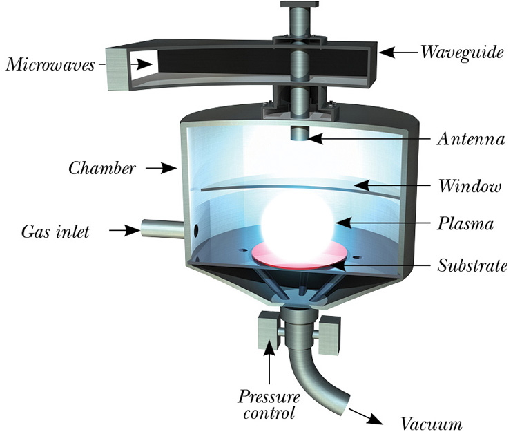
Fig. 1 — Microwave plasma assisted CVD diamond reactor.
Diamond Lapping, Polishing, And Laser Cutting
Synthesizing CVD diamond covers only half the engineering technology to manufacture the CVD diamond heat spreaders. Post-synthesis processing (Fig. 2) covers the other half. These steps involve rough and fine lapping of diamond substrates, followed by polishing and laser cutting of the material to its final specifications and shapes.
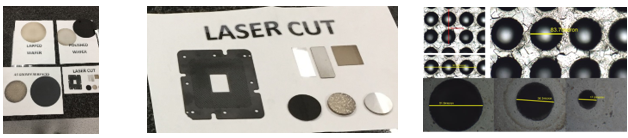
Fig. 2 — Examples of lapped, polished, and laser cut diamond wafers and specimens.
Laser machining of diamond is achieved through thermal ablation and/or laser-assisted chemical etching in oxygen or air. Laser drilling/cutting of diamond could be achieved in single or multi-step processes. It typically involves high-energy thermal conversion of the top surface to graphite, followed by ablation of converted graphite and forming of another thin layer of graphite. The thickness of this graphite layer depends on pulse duration and the thermal conductivity of diamond.
CVD Diamond For RF Packaging
In designing a system of thermal management, careful consideration of both the material and the application methodology is critical to minimize channel temperatures and extend the device’s lifetime. To date, the integration of SiC (400 W/mK) substrates with GaN has provided the best option for GaN HEMT and MMIC technology for high-power applications. However, despite the use of SiC substrate, adequate heat spreading remains the limiting factor in determining the maximum power dissipation for GaN based electronics.
As such, the path to long-term reliability is often achieved by de-rating the maximum power dissipation. A far better heat-spreading solution incorporating CVD diamond (2000 W/mK) has the potential for a factor of 3× or higher increase in power density, relative to current state-of-the art GaN devices. While GaN-based electronics are capable of delivering ultrahigh current and high power density, the failure of many high-end electronic systems is directly attributable to the lack of adequate thermal management (Fig. 3).
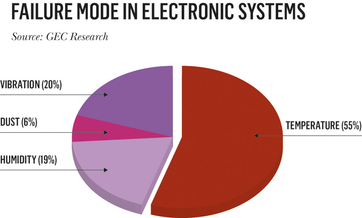
Fig. 3 — Cause of failure in electronic systems[3]
As an electrically conductive heat spreader, thick boron-doped diamond with 0.05 Ω-cm resistivity could be an ideal replacement for commonly used metal/diamond configurations, or other heat spreaders, such as copper, copper/refractory, or copper laminate. Mounting of RF/Microwave devices on BDD heat spreaders enables better isolation of the ground plane below 1.5 GHz and reduces the conductive losses above 1.5 GHz due to increased skin depth.
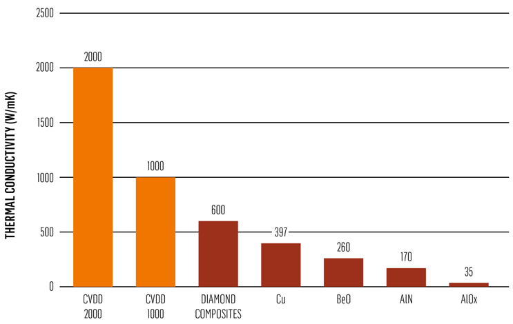
Fig. 4 — Comparison of CVD diamond with ‘traditional’ heat spreading materials
An Application Example
To demonstrate the practical impact of a diamond heat spreader, an RF amplifier design was analyzed. In this example, a vertical diffused metal oxide semiconductor (VDMOS) power amplifier package, designed with a Beryllium oxide (BeO) heat spreader on a Copper / Molybdenum (CuMo) flange, was analyzed for the impact of replacing BeO with diamond heat spreader. It should be noted that the main objective of the VDMOS user was lowering the system’s overall thermal resistance of the system, as well as avoiding the use of BeO due to its toxicity.
The CVD diamond heat spreader was found to have 30 percent lower thermal resistance when using a 0.300 mm-thick diamond spreader with thermal conductivity of 1000 W/mK (the original design used a 1.00 mm thick BeO heat spreader). The diamond heat spreader’s improved thermal resistance led to better linearity in RF performance and improved reliability due to reduced junction temperature. Fig. 5 depicts the impact of diamond heat spreader use on the temperature profile of junction-to-case for an optimal design.

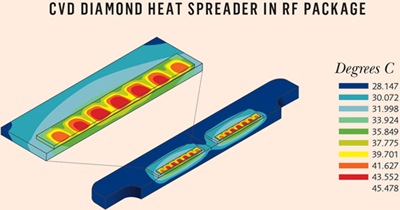
Fig. 5 — RF amplifier temperature profile thermal modelling.
The Cost Of Diamond
A subject worthy of an extended article by itself, the cost of a diamond heat spreader should to be considered from two different viewpoints. First, consider when standard heat spreaders cease to perform in cooling high power density devices in RF, microwave, and ASICs. Second, and potentially more important, is that the cost to improve performance could and should always be optimized multi-dimensionally. The ratio of device-to-spreader area, the spreader thickness, and the CVD diamond heat spreader thermal conductivity all play key roles in controlling thermal resistance and cost. As a result, it is imperative to follow a robust performance/cost model to optimize diamond heat-spreader benefits.
Summary
When comparing synthetic diamond against its ceramic counterparts, the former delivers benefits for a diverse range of industries and applications. This especially applies to thermal applications, where diamond thermal conductivity is far superior to other materials available on the market.
Significant improvements to electronic systems can be realized by using CVD diamond heat spreaders. Integration is relatively straightforward, as CVD diamond can be a direct replacement for aluminum nitride (AlN), BeO, or other advanced ceramics. Attention to detail at interfaces is important to keep overall thermal resistance low, and to optimize the effectiveness of the CVD diamond.
Through improved synthesis technology, advance processing, and ongoing cost reduction efforts, CVD diamond has become a crucial enabler as a heat spreader and heat dissipater for high power density RF applications. In line with the ever-increasing need for smaller and more powerful electronic devices and systems, including the growing demand for defense-related and 5G wireless applications, it is expected that this trend will continue in the years to come.
About The Author
Firooz N. Faili is the Principal Application Engineer for Thermal Products at Element Six, focused on developing new and sustaining existing products and markets. He has spent over twenty-five years on technology development at startups and established companies in semiconductor industry. He co-founded companies focused on developing GaN-on-diamond and novel CVD diamond growth technology. As a Principal Technologist at Varian Semiconductor, he worked on dielectric and conductor etch and CVD development; as Chief Technologist at LASA Industries, he was responsible for the development of a single cluster-tool methodology for multi-level metallization and prototyping of ASICs. He holds a BS and MS in chemical engineering, as well as a Ph.D. in material engineering.
[1] Collins Radio paper - “Development of Advanced Cooling Techniques and Thermal Design Procedures for Airborne Electronic Equipment, proposal submitted to United States Air Force Command, November 1968
The rule was adopted by applying Arrhenius equation. Damage/Time = A Exp( Ea/kT)
[2] For diamond and number of other semiconductors: http://matprop.ru/
For copper and copper composites: https://www.torreyhillstech.com/heatsinks.html
For silicon carbide: Rusheng Wei et al, “Thermal conductivity of 4H-SiC single crystals,” Journal of Applied Physics 113, 053503 (2013)
[3] Michael Reynell, “Advanced thermal analysis of packaged electronics systems using computational fluid dynamics technique,” Computer-Aided Engineering Journal, August 1990