
Si/SiGe Devices and The RF Communications Revolution

In the early 90's, it was thought impossible to take silicon bipolar junction transistors (BJTs) beyond the 10 GHz barrier. Designers thought III-V compound semiconductor materials would be the sole contributors to the RF communication revolution that we are experiencing today. The optimization of silicon bipolar design structures and the introduction of silicon germanium (SiGe) have retarded the anticipated transition to III-V materials for RF mixed-signal applications. The silicon research community has been closely tied to circuit design and is focused on scaling, resulting in impressive Si/SiGe HBT circuit speeds.
Table of Contents
Key Optimizations of Silicon Devices
SiGe HBTs Demonstrate Superior Performance
Emerging Applications for SiGe Devices
Key Optimizations of Silicon Devices
Strong efforts to reduce extrinsic parasitics have driven the optimization of Si device structures. The goal has been to maximize the cut-off frequency (FT) of the device by minimizing the emitter-base and collector-base depletion  layer capacitances as well as the forward transit time. Self-aligned single-polysilicon (SP) and double-polysilicon (DP) advanced structures have been effective because of their small parasitic capacitances. Base transit time, the key component of forward transit time, is diminished by reducing the intrinsic base width. Reduced transit time comes at the expense of intrinsic base resistance and Early voltage (VA). Improved isolation techniques such as shallow (STI) and deep trench (DTI) isolations have helped minimize collector-substrate capacitances by cutting straight through the NPN's subcollector area.
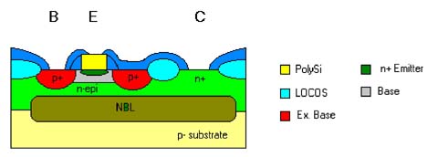
SP silicon bipolar transistor
A polysilicon emitter contact was the first of a series of major improvements to silicon devices. It helped increase emitter efficiency by suppressing the base-emitter hole current. This addition also allowed shallower emitter junction depths, permitting smaller base widths. These in turn led to smaller base transit times and an exponential increase in cut-off frequencies. Heavily doping the polysilicon emitter gives the devices low series resistance while maintaining adequate emitter-base breakdown voltages.
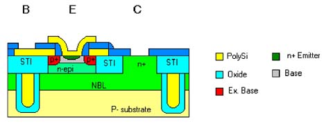
DP silicon bipolar transistor
The DP structure uses polysilicon contacts for both the emitter and base. Its architecture allows the base to be contacted over the field oxide. The extrinsic base junction area is contacted through polysilicon instead of metal. This reduces the active base area and diminishes the collector-base capacitance, increasing device speed. The self-alignment (SA) scheme, where the extrinsic base is self-aligned to the emitter edge, is usually preferred for performance considerations. The SA technique's main advantage is due to the sidewalls: the emitter stripe width is actually less than the minimum lithographic feature size, further reducing base-collector parasitic capacitances.
SiGe HBTs Demonstrate Superior Performance
SiGe HBTs replace the Si-implanted base of Si bipolar junction transistors (BJTs) with an epitaxially grown SiGe base layer, adding process complexity and increasing costs, but permitting a tremendous boost in speed. Grading the SiGe base through bandgap engineering gives a drastic increase in the electric field gradient across the junction. Electrons accelerate to a greater speed, reducing base transit time. The germanium (Ge) graded base region reduces the diffusion capacitance while the presence of Ge at the emitter-base junction promotes better injection efficiency. The higher the Ge doping in the base layer, the lower the base resistance. The Ge content is limited to 30% due to strain and lattice relaxation issues. Aside from being faster, these devices exhibit larger current gains, higher Early voltages (VA) and lower 1/f noise figures (NF).
Pioneered by the Institute for Semiconductor Physics (IHP; Frankfurt, Germany) SiGe:C technologies are currently very appealing. Incorporation of carbon in the SiGe base suppresses boron outdiffusion, increasing the allowed boron concentration in the base layer. Four main flavors of processes allow SiGe HBTs to reach the 50-100 GHz level .
Discrete SP and DP silicon BJTs dominate the 5-25 GHz and 20-50 GHz range respectively, while SiGe HBTs can reach speeds of 50 GHz and beyond. SiGe HBT's dominate Si BJTs with a 50% superiority in sheer speed alone, and are becoming more affordable with their increased commercialization. Although these HBT devices can exhibit maximum oscillation frequencies (Fmax) well in excess of 75 GHz, engineers can trade excess speed for reduced power consumption by decreasing the operating currents. In practice, this approach lets the RF communications industry provide extended talk/stand-by time for the digital European cordless telecommunications (DECT), GSM (900 MHz) and digital communications systems (DCS)/ personal communications systems (PCS) 1.8/1.9 GHz wireless voice and data phones.
A year after SiGe first went into commercial production with the two main SiGe foundries, IBM and TEMIC, many companies including GaAs manufacturers (RF-Microdevices, Alcatel, M/A-COM) are now licensing SiGe process technology or using SiGe epitaxy foundry services. Si/SiGe devices are far cheaper to manufacture than III-V based devices and benefit from their ease of integration with CMOS. The wireless communications sector is driving the SiGe integration, promoting single-chip integration of SiGe RF bipolar with CMOS silicon. These SiGe RF BiCMOS chips target low cost, high-speed multimedia wireless communication links to networks.
Emerging Applications for SiGe Devices
SiGe RF ICs are finding applications in the automotive, navigation/aerospace and communications sectors. SiGe has already claimed a large portion of the Bluetooth (2.4 GHz) market.
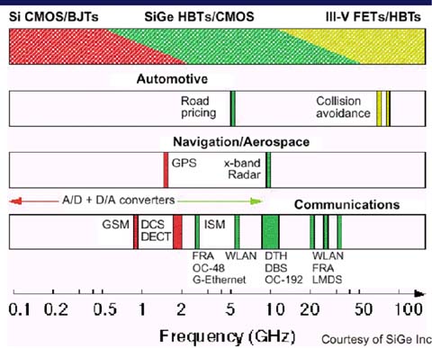
SiGe allows operating frequencies that are 2-3 times higher than silicon, and has larger current gain, output conductance, temperature stability and lower noise margins. It is being used for analog components such as low noise amplifiers (LNAs), power amplifiers (Pas), intermediate frequency mixers (IFs), voltage-controlled oscillators (VCOs), phase-locked loops, and analog-to-digital / digital-to-analog converters (ADC/DAC).
As SiGe becomes mainstream and its process technology matures, it may find future applications in optoelectronics superlattice structures or avalanche photo-diode photodetectors. Researchers are studying the use of SiGe as a pseudo-substrate for III-V compounds, so as to promote integration of GaAs-based devices onto silicon.
About The Author
Phillip Espinasse is a process development engineer involved in the research and development of RF c-BiCMOS technologies at PolarFab, a US-based mixed-signal IC foundry. He is also a writer for OE magazine, a monthly SPIE publication, a science and technology columnist for Photonics Online (www.photonicsonline.com) , and a member of the Semiconductor Online advisory board.
Phillip B. Espinasse
PolarFab
Technology Development Department
2800 E. Old Shakopee Rd.
Bloomington, MN, USA
Tel: (952) 876-3183
Fax: (952) 876-1683
e-mail: espinassep@polarfab.com