Role Call: Senior Staff Packaging Engineer

Does fear of the unknown keep you up at night? Are you unsure where your career in the RF/microwave industry is headed? Do you find yourself wondering what a certain job entails, how much you have to know, or what experience you might need to get started?
Role Call, a series on RF Globalnet, takes a “peek behind the curtain” to help answer the questions related to different jobs and career paths in the RF and microwave industry.
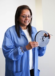
Recently, Mumtaz Bora, Senior Staff Packaging Engineer at pSemi, took time to answer some questions about her occupation. You might say that engineering is her calling. Since 2009, Mumtaz has grown in her role as a senior and staff packaging engineer at pSemi. Before that, she held positions as an advisory engineer and quality engineer. Mumtaz has experience with a variety of products and design methods, which have strengthened her skills in areas like factory DPPM reduction, supplier quality systems audits, interconnect technologies, failure analysis, and industry standards.
What does your position as a senior staff packaging engineer currently entail?
My position as a senior staff packaging engineer requires prototyping new packages and coordinating the technology transfer of the assembly processes to volume production. I cost-size the package prototypes, evaluate the package-assembly process, analyze the packages’ internal structures, and prepare the supporting documentation to enable our overseas subcontractors to build them. I also manage the yield improvements, corrective actions, process controls, and reliability monitoring of the packages built in our manufacturing facilities.
What education/certifications are required for this position, and what are the continuing education/certification requirements?
A bachelor’s or master’s degree in engineering (packaging, mechanical, electrical, material, or chemical), physics, or chemistry is required. The continuing education requirements involve learning design tools like AutoCAD, thermal modeling software like ANSYS, basic statistics, design of experiments, failure analysis, Six Sigma methodology, and how to document work instructions. Personally, I earned bachelor’s degrees in chemistry and biochemistry, and a master’s degree in interactive telecommunications.
Is training in chemistry or biochemistry a traditional pathway to this role? How has your educational background helped or hindered you in ascending to this position?
Chemistry and biochemistry are not traditional pathways to a packaging career, but my educational background, along with my industry background of PC board manufacturing for surface mount assembly, has helped me better relate to our customers’ issues. My knowledge of chemistry helps me understand the materials and the processes used in making packages — such as plating, etching, sputtering, and soldering. My biochemistry knowledge is valuable in understanding the environmental regulations, such as RoHS/REACH, and medical product application requirements. My graduate degree in interactive telecommunications broadened my knowledge of mobile product applications and the supply-chain requirements of successful volume manufacturing. Finally, my materials knowledge gives me insight into how RF losses impact the end product — for example, how the smoothness or roughness of copper traces affects the RF design, or how underfill applied on flip-chip bumps impacts RF performance.
What experience did you need for your position? How long did it take you to reach the skill level that you are at now?
Before working in packaging at pSemi, I worked in the computer industry and in cell phone manufacturing. This background helped me in understanding solderability, paste materials, cleaning issues, and the package-assembly process. At pSemi, I support assembly of ceramic and plastic packages. I was flexible in learning the package roadmap, product testing, and failure analysis. It took me three years to acquire the skill level needed to support wire-bond and flip-chip packages for high-reliability, aerospace, defense, automotive, and mobile-wireless applications.
What types of things did you need to learn on the job?
On the job, I learned process flows and how to inspect product in the backend operations where we thin and dice the wafers. I had to learn to create bills of materials (BOMs) for wire-bond and flip-chip assembly. The assembly BOM includes the release of the assembly drawings, package outline drawings, and the bond diagrams. I also had to learn wafer manufacturing processes. For commercial products and plastic packages, I had to become familiar with the JEDEC packaging standards. For high-reliability products, I had to learn the test methods in MIL-883 and MIL-PRF-38535. As a packaging engineer, I can affirm that knowledge of industry standards is an important asset in performing your job.
How do you spend a typical workday?
A typical workday involves looking at package drawings, reviewing qualification reports, conducting experiments for solderability, inspecting packages, and conducting failure analysis. Our packaging team also supports the cross-functional product teams for new product launches. This collaboration requires providing technical direction for package-material selection, package size, cost tradeoffs, and assessing supplier capabilities.
What are the biggest personal/professional challenges that your work presents for you?
Wire-bonded and flip-chip packages have their own unique assembly challenges. It is a tremendous professional challenge to ensure our development processes are robust, and [to] assist our subcontractors in fine-tuning their processes to achieve good yields and reliability. Also, keeping projects on-track and avoiding unexpected technical issues is a constant challenge. On a personal level, I am challenged daily to respond to technical issues that our customers and subcontractors face. But, by working together, we can quickly resolve these challenges, enabling our subcontractors and customers to move forward in a timely manner.
What specifically drew you to this career path?
In my undergraduate years, I considered a career in medicine, but I changed my path after a temporary assignment at IBM in PC board manufacturing. I was amazed at how many chemical operations it takes to make a PC board. I got really interested in electronic packaging and decided to pursue a career in packaging. A big draw for me is the ability to see a project through from start to finish. I enjoy working on projects from initial start to production release and being involved with all aspects of the project.
What is your favorite part of your occupation?
My favorite part of my occupation is working with cross-functional teams and subcontract facilities to make packages that are more cost-effective, lighter, smaller, and more reliable, while also meeting the demands of the pSemi customers and the RF/microwave industry. Improvements in packaging can only be achieved with good partnerships, shared knowledge, and teamwork with our subcontractors. I also enjoy applying the knowledge of materials, processes, and manufacturing to resolve manufacturing-yield situations, and driving our subcontractors to a control system that prevents issues from occurring, rather than being in a reactive mode of addressing crises.
What tools or programs do you use for new and existing packaging designs, and why? Are there any other tools, equipment, or programs that you use in a design process?
At pSemi, we use several design tools for chip design and PCB design, such as Cadence, Virtuoso, Allegro, Zuken; we use modeling software, such as ANSYS and AutoCAD, for generating the package outline drawing. We use a variety of test equipment to characterize packages. We also use SEM/EDX- and FIB techniques for package-assembly characterization and for failure analysis.
What would be on your “wish list” for technologies, services, or resources that could improve your job performance or make your work easier, and why?
My “wish list” includes the use of innovative technologies — such as nanomaterials and photolithography techniques — that can form ultrathin circuits to make semiconductors smaller and faster, enabling more powerful IoT/wireless solutions. At pSemi, our goal is to simplify the volume manufacturing processes and improve efficiency. Turn-key design and manufacturing services are ideal to accelerating development cycles. A well-trained workforce is an asset because our success depends upon our ability to build and test the product to meet customer requirements. Clear, concise documentation from all teams is essential to avoid redo and misinterpretations. Finally, my work with overseas facilities requires overcoming cultural and language barriers, so having a liaison available to assist with the transition is very helpful. I am fortunate that our parent company, Murata, and many of our subcontractors have liaisons available.
We all have interests that are separate from work. What hobbies or other interests do you have outside the office?
My hobbies include traveling, meeting new people, and learning about different cultures and civilizations. I also enjoy creative artwork, nature walks, and community-service projects.
What advice would you give to an individual just starting out in this field, both in terms of component design and professional development?
My advice is to apply the theoretical knowledge to the designs and further optimize designs through modeling, data collection, good observation, and reliability testing.
For professional development, industry participation is very important to see packaging trends and understand how others are solving similar problems. Participating in professional societies and sharing knowledge via technical paper presentations or chairing sessions is helpful for professional growth. I recommend membership in professional societies, such as Surface Mount Technology Association (SMTA), International Microelectronics Assembly and Packaging Society (IMAPS), Institute of Electrical and Electronics Engineers (IEEE), and Institute of Electronic Packaging and Interconnection (IPC). I am very active in these professional societies and, over the years, I have organized events, spoken at industry events, and served in various leadership positions. These organizations open up many opportunities and prepare engineers for the factories of the future.
I also encourage students or young professionals to seek out a mentorship. SMTA has an email mentoring program through MentorNet. You can also connect with me on LinkedIn; I’d be happy to answer your questions.
...
If you’ve ever wondered what a day in your RF dream job looks like, or you just want to discuss a job you’re passionate about, contact the author at mstonefield@vertmarkets.com with story suggestions, or to volunteer as a Q&A subject.
About the Author:
 Marissa Stonefield is a Web Content Specialist for Photonics Online, RF Globalnet, and Med Device Online. She graduated from Messiah College with a B.A. in marketing, and from the Community College of Beaver County with an A.B. in business administration. She has previously worked as a content writer for Vanko Trading Inc., and as a journalist for Examiner.com, and Weddings Year Round Magazine in Lancaster, Pa.
