
pSemi Announces World's First Monolithic, SOI Wi-Fi Front-End Module

Ideal for Wi-Fi Home Gateways, Routers and Set-top Boxes, the 2.4 GHz FEM Uses a Smart Bias Circuit to Deliver a High Linearity Signal and Excellent Long-packet Error Vector Magnitude (EVM) Performance
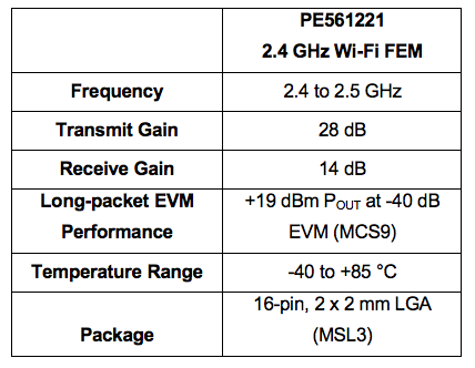
SAN DIEGO – pSemi Corporation (formerly Peregrine Semiconductor), a Murata company focused on semiconductor integration, introduces the world’s first monolithic, silicon-on-insulator (SOI) Wi-Fi front-end module (FEM)—the PE561221. Ideal for Wi-Fi home gateways, routers and set-top boxes, this high-performance module uses a smart bias circuit to deliver a high linearity signal and excellent long-packet error vector magnitude (EVM) performance. The PE561221 combines the intelligent integration capabilities of pSemi’s SOI technology and Murata’s expertise in Wi-Fi connectivity solutions and advanced packaging. This 2.4 GHz Wi-Fi FEM integrates a low-noise amplifier (LNA), a power amplifier (PA) and two RF switches (SP4T, SP3T). The monolithic die uses a compact 16-pin, 2 x 2 mm LGA package ideal for either stand-alone use or in 4 x 4 MIMO and 8 x 8 MIMO modules.
“The new IEEE 802.11ax standard is utilizing high-order modulation schemes (1024 QAM) with demanding EVM requirements,” says Colin Hunt, vice president of worldwide sales at pSemi. “Traditional process technologies struggle to keep up with both performance and integration requirements, and only SOI can offer the ideal combination of integration and high performance. This new monolithic Wi-Fi module is a great example of the types of technology and product advancements pSemi and Murata can accomplish together.”
The 2.4 GHz Wi-Fi FEM is based on pSemi’s UltraCMOS® technology platform—a patented, advanced form of SOI. With its outstanding RF and microwave properties, SOI is an ideal substrate for integration. When paired with high-volume CMOS manufacturing—the most widely used semiconductor technology—the result is a reliable, repeatable technology platform that offers superior performance compared to other mixed-signal processes. UltraCMOS technology also enables intelligent integration—the unique design ability to integrate RF, digital and analog components on a single die.
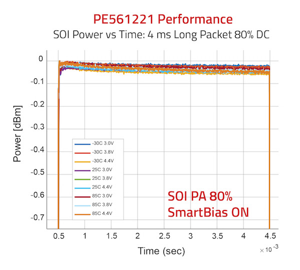
The PE561221 uses a smart bias circuit to deliver a high linearity signal and excellent long-packet EVM performance.
Features, Packaging and Availability
The PE561221 leverages the intelligent integration capabilities of UltraCMOS technology to deliver exceptional performance, low power consumption and high reliability with 2 kV HBM ESD rating. Through advanced analog and digital design techniques, the Wi-Fi FEM delivers excellent long-packet EVM performance with less than 0.1 dB of gain droop while operating across the entire -40°C to 85°C temperature range. At -40 dB EVM (MCS9), the output power is +19 dBm with less than 0.05 dBm droop in power output after a 4 milliseconds packet. The IC delivers best-in-class dynamic error vector magnitude (DEVM) and current consumption without requiring digital pre-distortion (DPD), and it has excellent MCS11 performance for 802.11ax applications.
Volume-production parts and samples of the PE561221 are available from pSemi. For sales information, please contact sales@psemi.com.
The PE561221 is the first product in the pSemi Wi-Fi FEM portfolio; the product roadmap includes 5 GHz Wi-Fi FEM solutions.
About pSemi
pSemi Corporation is a Murata company driving semiconductor integration. pSemi builds on Peregrine Semiconductor’s 30-year legacy of technology advancements and strong IP portfolio but with a new mission: to enhance Murata’s world-class capabilities with high-performance RF, analog, mixed-signal and optical solutions. With a strong foundation in RF integration, pSemi’s product portfolio now spans power management, connected sensors, optical transceivers antenna tuning and RF frontends. These intelligent and efficient semiconductors enable advanced modules for smartphones, base stations, personal computers, electric vehicles, data centers, IoT devices and healthcare. From headquarters in San Diego and offices around the world, pSemi’s team explores new ways to make electronics for the connected world smaller, thinner, faster and better. To view pSemi’s semiconductor advancements or to join the pSemi team, visit www.psemi.com.
###
The Peregrine Semiconductor name, Peregrine Semiconductor logo and UltraCMOS are registered trademarks and the pSemi name, pSemi logo, HaRP and DuNE are trademarks of pSemi Corporation in the U.S. and other countries. All other trademarks are the property of their respective companies. The pSemi website is copyrighted by pSemi Corporation. All rights reserved.
Source: pSemi