
Power Amplifier MMICs For mmWave 5G
By Liam Devlin, Stuart Glynn, and Graham Pearson, Plextek RFI

As the development effort focused on mmWave 5G continues to grow, component suppliers are busy developing new products that they hope will see deployment in high volume commercial systems. This article looks at the semiconductor process and SMT packaging options for the realisation of power amplifier (PA) integrated circuits (ICs) operating at millimeter wave (mmWave) frequencies. It also presents examples of 5G mmWave SMT packaged PA designs.
The preferred operating bands for mmWave 5G are starting to become apparent. In the US, licensed bands at 28 GHz (27.5- 28.35 GHz), 37 GHz (37-38.6 GHz), and 39 GHz (38.6- 40GHz) are being deployed in the first trial systems. More recently, plans to auction spectrum at around 24 GHz (24.25-24.45, 24.75-25.25 GHz) have been announced. In Europe, the Radio Spectrum Policy Group (RSPG) has recommended the 26 GHz band (24.25 - 27.5 GHz) as the pioneer band for 5G [1], with all EU member states making a portion of this band available for 5G.
Technology Choice
There is much debate about the best choice of semiconductor technology, required output power per PA, and the optimum number of transmit channels. Table 1 compares the key solid-state processes currently being used for mmWave 5G PAs. The saturated RF output power column is not an attempt to provide a theoretical maximum limit for each technology; it is an indication of what the authors currently consider to be a practical limit for a single die commercial PA using the various technologies. It can be seen that, as output power capability increases, so does cost per unit area. However, the power density per unit gate width from the active devices also increases, so that a 2W PA on a GaN process (for example) would be smaller than a 2W die on a GaAs PHEMT process.
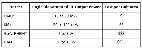
Table 1 — Comparison of solid state processes for mmWave 5G power amplifiers
High-volume automated assembly requires the availability of components in SMT-compatible packages. A range of practical packaging technology options have been demonstrated for SMT packaged mmWave PAs, and these are summarised in Table 2. The upper frequency in the table is not a hard limit; it is a practical frequency to which commercial products have been readily demonstrated.
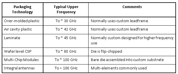
Table 2 — Comparison of SMT packaging technologies for mmWave 5G power amplifiers
Fig. 1 depicts a 28 GHz PA IC developed by Plextek RFI. It was designed for 5G applications across an operating band of 26.5 to 29.2GHz. It was realized on a 0.15µm gate length enhancement mode (E-mode) PHEMT process, which means it does not require a negative supply to set the gate bias. The PA was housed in a 4mm x 4mm 20-pin overmolded plastic QFN package. A custom leadframe was designed to optimize the performance, but it used a standard, high-volume overmolded packaging process. The evaluation PCB process shown in the photograph also was designed by Plextek RFI. The substrate material was a low-cost laminate: Rogers RO4003, substrate thickness 8 mil. To reference measured data to the ports of the packaged device, a Thru-Reflect-Line (TRL) calibration PCB was realized on the same substrate material.
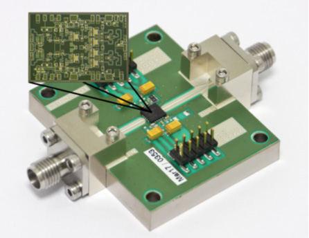
Fig. 1 — Evaluation PCB for the SMT packaged 28 GHz 5G PA
The PA is a three-stage design with an on-chip, temperature-compensated output power detector. The output stage uses four power-combined transistors. When designing mmWave PAs, the choice of transistor size is a tradeoff between RF output power and available gain. As the transistor size increases, so does the maximum RF output power it can deliver, but the increased parasitics reduce the available gain. For a multi-stage design, the impact of low stage gain on overall efficiency can be significant. The driver stage makes use of two transistors, each driving two of the output devices, and a single transistor is used for the input amplification. Bias decoupling components have been included on-chip, together with appropriate low frequency stabilisation networks, to ensure broadband unconditional stability.
PAs for 5G applications need to operate backed-off from compression to maintain modulation fidelity. The design was optimized for optimum linearity and Power Added Efficiency (PAE) with third-order intermodulation products below -35dBc — this was found to be around 7 dB, backed-off from 1 dB compression. To meet this requirement, the transistors were biased in relatively deep Class AB. As the transistors were biased more toward Class B, the efficiency improved, but the gain and linearity both decreased. Significant effort was expended during the early part of the design process undertaking load-pull simulations to select the optimum bias point and transistor geometries.
Accurate EM simulation is vital if the performance of mmWave ICs is to be accurately predicted [2]. Careful EM simulation and optimization of the PA layout was undertaken. The design and EM simulation took account of the packaging parasitics, and performance was optimized for the packaged part assembled onto the PCB.
Fig. 2 shows the measured S21 and S11 (solid traces) compared with the simulated values, which are denoted by the dashed traces. Both the measured and simulated data include the effects of the package lead-frame, the bondwire, the molding compound, and the PCB. Agreement between the measured and simulated performance data is very good, with the measured response being just slightly higher in frequency. The quiescent bias for the amplifier was +4V Vdd and 182 mA Ids. Small-signal gain is just over 20 dB from 26.5 GHz to 29.5 GHz, and the S11 is below -16 dB. The output was matched for optimum linearity at back-off, rather than for a conjugate match, but the S22 (not shown) is still around -10 dB across the same band.
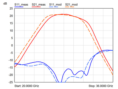
Fig. 2 — Measured to modelled (simulated) s-parameters of the SMT packaged 28 GHz PA
The RF output power at 1 dB compression (P-1dB) was around 26 dBm with a PAE of around 30 percent. The measured third order intercept point (IP3) was 32 dBm to 33 dBm, varying little across the band. A comparison of the measured to simulated PAE versus RF output power at 29.2 GHz (the top of the design band) is plotted in Fig. 3. The design was optimized for operation at around 7 dB back-off (RF output power of 19 dBm), and excellent agreement between measured and simulated performance is demonstrated in this region. The PAE at 7 dB back-off was between 7 percent and 9 percent, depending on operating frequency.
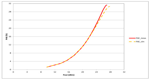
Fig. 3 — Measured to modelled large signal performance of the SMT packaged PA at 29.2 GHz
Fig. 4 depicts a 37-42 GHz PA (so, simultaneously covering the 37 GHz and 39 GHz 5G bands). It is a higher-power part than the 28 GHz PA described above, having a P-1dB of around 31 dBm, and was realized on a 0.15µm depletion mode (D-mode) PHEMT process. It is also housed in an SMT QFN plastic package with a custom leadframe, but it makes use of an air cavity, rather than the overmolded plastic approach used for the 28GHz PA.
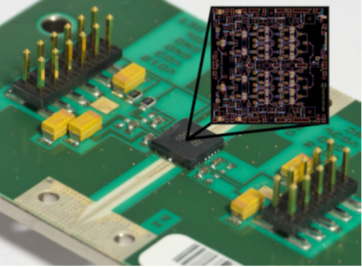
Fig. 4 — Photograph of 39GHz SMT packaged PA evaluation PCB with die layout
The evaluation PCB uses the same low-cost laminate material as the 28 GHz part (Rogers RO4003, with an 8 mil substrate thickness). The PCB area for attachment of the QFN package paddle incorporates a dense array of copper-filled vias. This ensures low inductance grounding (essential for good RF performance on mmWave amplifiers) and improved thermal conductivity. The measured results presented below are for the packaged part assembled onto the representative evaluation PCB. All results are referenced to the package ports.
The 39 GHz PA is a 4-stage amplifier with an on-chip, temperature-compensated output power detector. Eight power-combined transistors are used in the output to achieve the higher RF output power. Stage 3 uses eight smaller transistors to drive the output stage; stage 2 uses four transistors; and the input stage has two transistors. The available gain of the 0.15 µm transistors drops with increasing frequency, and this 4-stage design has a similar gain to the 28 GHz 3-stage design described above (~ 20 dB).
Fig. 5 shows the measured power transfer characteristics at 39 GHz. Supply current (green trace) can be seen to rise as the amplifier is driven harder. The output P-1dB point is 31 dBm, and the saturated output power (at P-2dB) is 32 dBm. The measured IP3 is plotted against frequency in Fig. 6 ,and is a relatively flat 40 dBm from 37 GHz to 42 GHz.
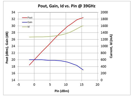
Fig. 5 — Measured power transfer characteristics, 39 GHz SMT packaged PA
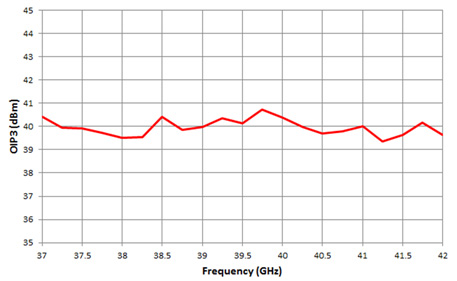
Fig. 6 — Measured IP3 versus frequency, 39 GHz SMT packaged PA
Our final 5G PA example targets the 26 GHz 5G Pioneer band. It is a three-stage amplifier designed on a commercially available 0.15 µm gate length D-mode PHEMT process. Like the 28 GHz and 39 GHz PAs described above, it includes an on-chip, temperature-compensated power detector to provide a measurement of the transmitted RF output power. The 3.5 mm x 1.2 mm MMIC die is shown in Fig. 7. A length of 50 Ω track is evident at the input, as the die was extended in the x-dimension to allow arraying as part of a multi-project mask set. A production version of the die would occupy 3 mm x 1.2 mm.
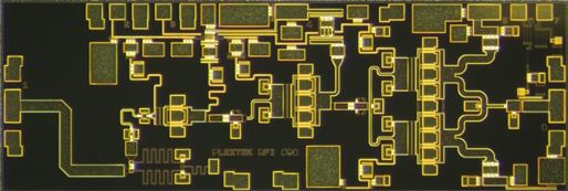
Fig. 7 — Photograph of the 26 GHz 5G pioneer band PA
The relatively modest RF power level (~ 26 dBm) targeted by this design meant that only two power-combined transistors were required for the output stage. Single transistors were appropriate for both the driver stage and the input stage. The sizes of the driver and input devices were selected carefully to ensure they would still be operating with good linearity as the output stage started to compress. This is crucial to ensuring the complete PA’s optimum linearity.
Linearity will be key for PAs used in 5G applications, so the amplifier was designed for optimum performance when operating 6 dB backed-off from compression (P-1dB). This requirement was inherent to the design process from the outset, and extensive load-pull simulations were undertaken using an accurate large-signal model to determine the optimum quiescent bias point for each transistor.
The PA was measured as a bare die using RF-on-wafer (RFOW) probing. A set of TRL calibration standards was fabricated on the same wafer as the PA to allow accurate calibration to the RF ports of the amplifier. Fig. 8 plots the RFOW-measured s-parameters of the PA die (solid traces) compared with the simulated S21. Excellent agreement between measured and modelled performance is evident. A measured gain of 22.5 dB ± 1 dB is demonstrated from 24 GHz to 28 GHz; across the same band, S11 is < -13 dB and S22 < -10 dB. Total quiescent current consumption, from all 3 stages, was 210 mA from a +6 V supply.
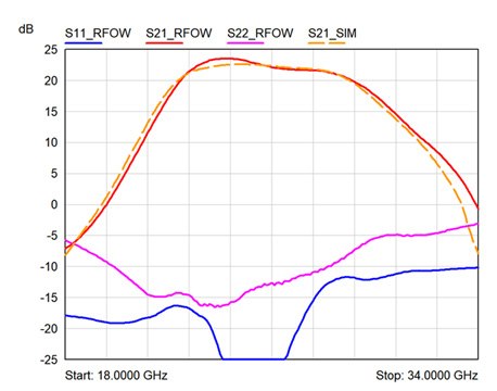
Fig. 8 — RFOW measured to simulated s-parameters of the 26GHz 5G pioneer band PA
A custom laminate SMT package was designed to house two of the die in a dual-channel arrangement. This is depicted in Fig. 9, along with a photograph of the QFN-style laminate package.
Fig. 9 — Custom dual-channel laminate SMT package for the 26 GHz 5G pioneer band PA
The package manufacture and assembly was undertaken by Filtronic, a UK manufacturer of custom RF, microwave and millimetre wave components and subsystems. The custom laminate package approach has two advantages over plastic QFN packages:
- The die sit in a pocket in the laminate material, so their surface is at a similar level to the lead to which the RF ports are bonded. This reduces the bondwire inductance.
- With a leadframe-based package, the size of the mmWave IC must be adjusted to ensure minimum bondwire lengths in the selected package style. With a custom laminate package, the package can be optimised for an existing design, regardless of the die dimensions.
One of the laminate-packaged dual-channel PAs assembled onto a laminate evaluation PCB is shown in Fig. 10. As with the packaged component measurements presented above, a TRL calibration approach was used to reference the measured data to the ports of the SMT package.
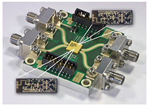
Fig. 10 — Evaluation PCB for the dual channel 26 GHz 5G pioneer band PA
Fig. 11 shows the measured s-parameters of both channels of one dual-channel packaged PA, compared with the RFOW measured s-parameters of a typical (but different) bare die IC. Both channels of the packaged PA have a very similar gain response (S21), despite the die not having been selected for close proximity on the wafer. The RFOW measured S21 (the dashed trace) is very similar to that of the packaged device. This agreement between SMT packaged part performance and RFOW performance clearly demonstrates the quality of the die to PCB transition provided by the custom designed laminate package.
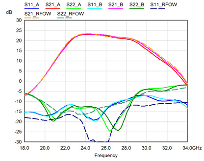
Fig. 11 — Measured s-parameters of both channels of a packaged 26 GHz PA, compared to RFOW (dashed trace)
The measured S22 of the packaged part is less than -12.5 dB from 24 GHz to 28 GHz, and the packaged part actually shows improved output match at the top of the band, compared to the bare die. A slight degradation in the measured S11 of the packaged part is evident compared with the bare die, but is still less than -10 dB.
The 26 GHz SMT-packaged dual-channel PA’s performance also was measured over temperature. The measured output IP3 is plotted in Fig. 12, for temperatures of -40°C, +25°C, and +85°C. At room temperature and at -40°C, the typical IP3 is around 36.5 dBm, which is around 10 dB higher than the P-1dB. At high temperature, the IP3 drops by around 1 dB, due in part to the falling gain of the driver stages with rising temperature[3].
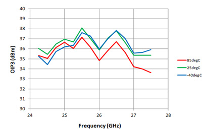
Fig. 12 — Measured IP3 (one channel) of a packaged 26 GHz PA over temperature
As 5G technology rolls out, the demand for high performance, low-cost PAs compatible with SMT assembly and high volume manufacture will increase. This article has looked at the semiconductor processes and packaging technologies that could be used, and has presented examples of mmWave 5G PAs designed by Plextek RFI. Looking to the future, as the 5G market matures, the demands on component suppliers will increase, with dual-band and multi-band PAs [4] likely to be required.
For more information on this topic, you can watch this video by Plextek RFI, which describes the development of a dual channel PA, housed in a custom laminate SMT package and covering the full 26 GHz 5G band.
About The Author
Liam Devlin is the CEO of Plextek RFI, a UK-based design house specialising in the design and development of RFICs, MMICs, and microwave/mmWave modules. He has led the design and development of over 90 custom ICs on a range of GaAs, GaN, and Si processes at frequencies from baseband to 90 GHz, and has also developed microwave and mmWave sub-systems using a variety of technologies. Liam previously worked as Chief Designer for Marconi Caswell, and was employed by Philips Research Laboratories. Liam has a BEng in Electrical and Electronic Engineering from the University of Leeds, UK.
References
- The EU’s Radio Spectrum Policy Group, “Strategic Roadmap Towards 5G for Europe”, November 2016 (http://rspg-spectrum.eu/wp-content/uploads/2013/05/RPSG16-032-Opinion_5G.pdf )
- Plextek RFI Closes the Gap between Measured and Modelled MMIC Performance (https://www.plextekrfi.com/wp-content/uploads/accurate_simulation_of_mmics.pdf )
- Stuart Glynn, Liam Devlin and Graham Pearson, “A Dual Channel SMT Packaged PA for 26GHz 5G”, Proceedings of the ARMMS RF and Microwave Conference, November 2018
- Stuart Glynn and Liam Devlin, “The Design of a Dual-Band PA for mm-Wave 5G Applications”, Proceedings of the ARMMS RF and Microwave Conference, November 2017