
Okmetic Showcasing High Resistivity Silicon Wafers For Superior RF Filter And Device Performance At Booth #347
Okmetic, the leading supplier of advanced silicon wafers for the RF market is showcasing its products at the International Microwave Symposium. Come meet our experts at booth #347 to discuss how our wafer solutions can enhance your RF device performance.
Okmetic is the leading supplier of advanced silicon wafers for the RF market. Our high resistivity RFSi® wafers improve RF device performance and Total Cost of Ownership, enabling more ambitious designs for RF filters and devices including BAW, TF-SAW, IPDs, GaN-on-Si Power amplifiers, switches, and antenna tuners.
Our RFSi® wafer portfolio in 150-200 mm includes:
High Resistivity SSP or DSP wafers
- Resistivities up to >10 kOhm-cm
- With or without highly efficient trap-rich layer
- Option for <700nm TTV
RF GaN Substrate wafers for GaN-on-SI applications
- Extra thick <111> MCz wafers
High Resistivity Bonded SOI wafers with or without cavities
Engineered High Resistivity wafers enabling minimal RF losses Our Engineered High Resistivity and Engineered Ultra High Resistivity wafers offer exceptional linearity and minimal losses in RF devices, thanks to their dual properties: high resistivity silicon mitigates bulk conductivity, while the trap-rich layer reduces surface conductivity. These properties are crucial for addressing the challenges presented by new 5G bands and higher frequencies, as they balance steep skirts, low insertion losses, and wide bandwidths in RF filters and devices.
Exceptional second harmonics using Engineered Ultra High resistivity wafer with trap-rich layer
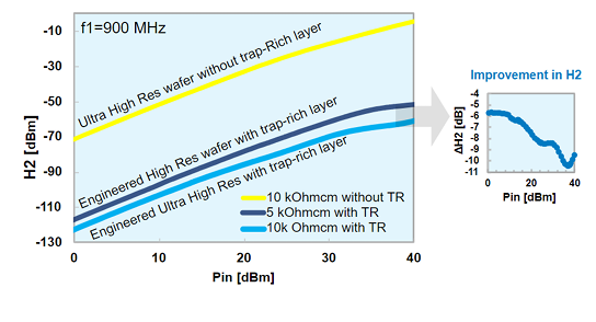
Measured with 2mm length 50Ω CPWs by Incize.
Our Engineered Ultra High Resistivity SSP and DSP silicon wafers, featuring resistivity over 10,000 Ohm-cm and an efficient trap-rich layer, are optimized for demanding RF filter applications. These wafers provide the highest effective resistivity, virtually eliminating substrate-induced losses and nonlinearities, and offering superior 2nd harmonic and intermodulation distortion (IMD) values.
RF GaN Substrate wafers offering advanced stress management and slip resistance
Power management in RF world uses thick <111> oriented high resistivity wafers as a platform for GaN-onSi applications. Our RF GaN Susbstrate wafers are designed to endure the extreme stresses of the RF GaN epi process and to drive the insertion losses lower, which makes them optimal platforms for Power management in the dense 5G base station network. This unique substrate option is manufactured with the Magnetic Czochralski crystal growth method and can’t be manufactured with the other commonly used crystal growth method Float Zone.
About Okmetic
Okmetic, founded in 1985, is the leading supplier of advanced silicon wafers for MEMS, sensor, RF, and power devices. The company’s extensive 150 to 200 mm wafer portfolio comprises comprehensive lines of High Resistivity RFSi® wafers, Power Device wafers, and MEMS wafers, including SOI, SSP, DSP, and Patterned wafers, TSV wafers, and GaN Substrate wafers.
Okmetic has a worldwide sales organization, and its headquarters are located in Finland, where the majority of its silicon wafers are manufactured. The company is currently building a fab expansion to more than double its production capacity. This fab expansion, focusing on 200 mm SSP and DSP wafers, is set to be operational in early 2025. Learn more about Okmetic at www.okmetic.com.
Come visit our booth #347 or pre-book an appointment:
Galya Stoeva
Vice President, Sales North America
galya.stoeva@okmetic.com
+1 9254814854
Petri Santala
Senior Manager, Technical Customer Support
petri.santala@okmetic.com
+1 4697771875