
Boron-Doped CVD Diamond As An Electrically Conductive Heat Spreader In RF/Microwave Applications
By Firooz Faili, Element Six Technologies

Doping with boron during chemical vapor deposition (CVD) synthesis allows for the growth of electrically conductive diamond. Some important applications of boron-doped diamond (BDD) include chemically resistive electrodes and electrically conductive thermal management material (~700 W/mK), whilst the conductivity allows the diamond to be cut by the electrical discharge machining method. The boron concentration influences thermal conductivity and electrical resistivity. Understanding how boron doping influences these properties is the key to successful integration of the material for various applications.
As an electrically conductive heat spreader, thick BDD with metallic conductivity (0.05 Ω-cm resistivity) is an ideal replacement for commonly used heat spreaders such as copper, copper/refractory, or copper laminate. Mounting RF/microwave devices on a BDD heat spreader enables better isolation of the ground plane below 1.5GHz, and results in a reduction of conductive losses above 1.5GHz due to the increased skin depth.
For electronic applications, operating below 1.5 GHz, the standard metallized heat spreader may introduce unwanted coupling between ground planes, contributing to signal distortions and capacitive coupling of ground planes. In this region, it is functionally beneficial to sacrifice some of the ultra-high thermal conductivity of diamond by making it electrically conductive.
Boron-Doped Diamond Resistivity And Thermal Conductivity
For microelectronic packaging applications, an ideal heat spreader would combine superior thermal properties with RF conductivity. BDD is uniquely positioned to deliver the advantage.
Thermal conductivity and the resistivity of BDD was measured on a collection of specimens. SIMS (Secondary Ion Mass Spectrometry) was used to measure the boron concentration [3]. The electrical resistivity of each specimen was measured using Van der Paw structures.
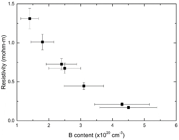
Fig. 1 — Measured electrical resistivity versus boron concentration
BDD thermal conductivity was measured using a laser flash technique (Fig. 2), which makes use of a short, high-energy, laser pulse of approximately 8 ns in duration [4]. The pulse impinges on one face of the diamond plate. The temperature rise on the opposite face is measured using a fast (20 MHz), far-IR point photovoltaic detector. This is recorded by a digital storage oscilloscope, from which the thermal diffusivity and subsequent thermal conductivity is calculated.
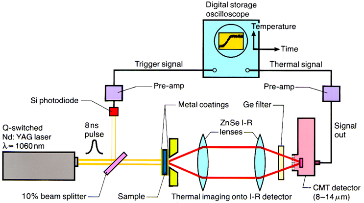
Fig. 2 — Laser-flash setup and methodology
In theory, any point on the temperature rise curve can be analyzed to yield D (Thermal Diffusivity):
Equation 1: D = WxL2 / π2tx
Where L is the test piece thickness, tx is the time for the test piece to reach a fraction of the maximum temperature, x is the fraction of the maximum rise in temperature, and Wx is a constant in the absence of radiation loss and finite pulse corrections.
The thermal conductivity is then calculated using:
Equation 2: TOC \h \z \c "Equation" k=DCpρ ![]()
Measured and calculated values for electrical resistivity and thermal conductivity of BDD are the verification of suitability of this material for advanced RF packaging applications.
Measured And Modelled Thermal Conductivity (Callaway-Holland Model)
Mathematical modeling is an essential part of the design and development of most systems. Materials and material systems are not precluded from modeling. The combination of modeled trends and verified measured data confirms the credibility of assumed boundary conditions and validity of the model.
Plots of thermal conductivity versus boron concentration were created from the set of measurements (discrete points) and were combined and plotted against a Calloway-Holland model (line) for predicting the thermal conductivity (Fig. 3).
The Callaway-Holland method has been used extensively for analysing the thermal conductivity of diamond [5]. The model accounts for phonon-phonon scattering, as well as scattering caused due to point defects (substitution impurities, interstitial impurities, and vacancies) and extended defects (dislocations and grain boundaries).
The closely correlated measured data and model trend is an indication of the understanding and predictability of BDD as a viable material.
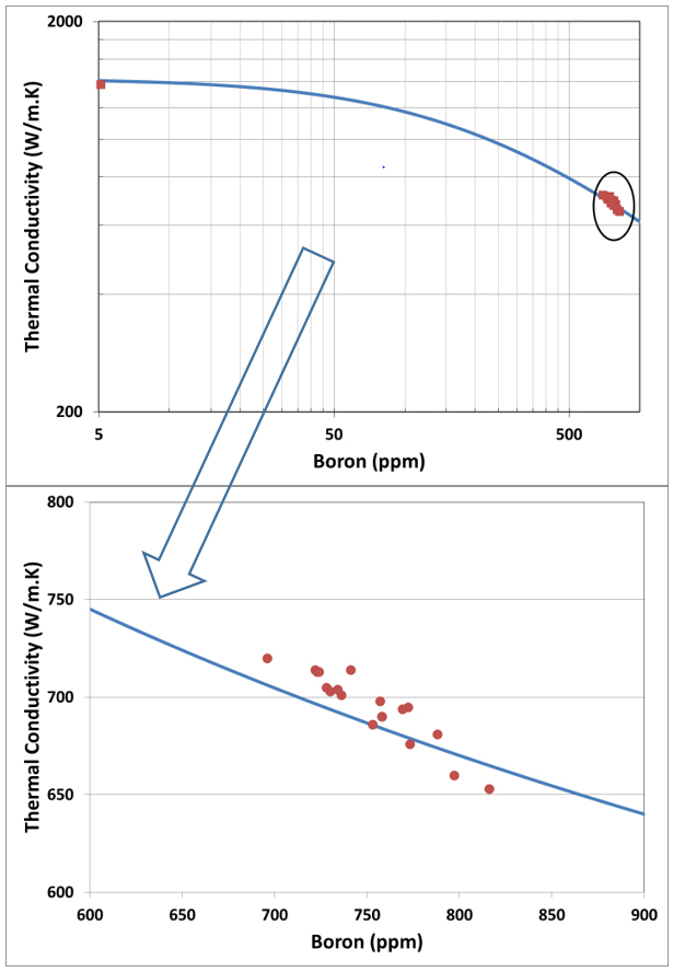
Fig. 3 — Combined plot of measured and modelled thermal conductivity versus boron concentration
Heat Spreader For RF Applications
When facing heat flux from high power density hot spots in optoelectronics — for example, in RF high-power amplifiers (HPAs) — the inclusion of CVD diamond in the packaging delivers improved reliability and increased power handling.
Typically, electronic devices — especially HPAs and monolithic microwave integrated circuits (MMICs) — are mounted on a flange requiring 1) high thermal conductivity to spread out the heat generated in the die, 2) low coefficient of thermal expansion (CTE) mismatch with the die to minimize residual stress, and 3) a noise-free ground plane for the transmission lines in the die.
It should be noted, to provide a good electrical connection and noise-free grounding, undoped diamond must be metallized with a metal stack typically terminating with 3 to 4 mm of gold [6].
Skin Effect
RF current flows on a metal surface, for typical metals (Cu or Au), above 1.5 GHz. The already very thin skin depth continues to decrease as RF frequency increases. The decrease in skin depth results in a surface resistance increase, as well as increasing conductive losses [7]. Above 1.5 GHz, in comparison to Cu and Au, BDD has nearly two orders of magnitude larger skin depth at the same RF frequency (Fig. 4). The higher conduction cross-section of BDD not only enables better RF performance by improving the ground-plane isolation, it also reduces conductive losses at higher frequencies.
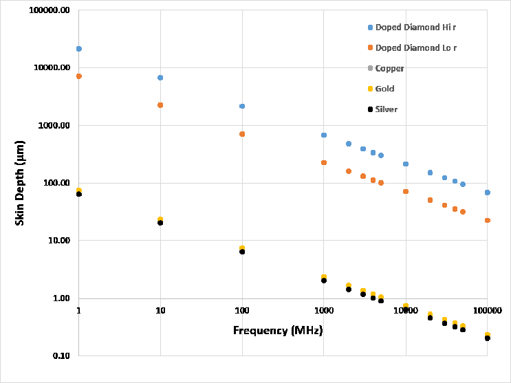
Fig. 4 — Skin depth for conductors at increasing operation frequency
The minimum thickness at which a thin layer of metal carrying an RF signal behaves as an infinitely thick piece of metal is at around twice the skin depth [8]. Above 1.5 GHz, the skin effect dominates, and there is no difference between an infinite thick layer of gold and a 4 mm thick gold layer on top of a dielectric. This was clearly demonstrated by Zhang et al [8]. They used two transmission structures, the TFMSL (thin-film micro-strip line) and MIMI (metal–insulator–metal–insulator), to study the influence of embedded thin-film metallization layers, normally designed as ground planes, upon the dispersive characteristics of multilayer micro-strip lines (Fig. 5). The implication of this finding is that, at higher frequencies, using BDD will reduce losses due to conduction cross section.
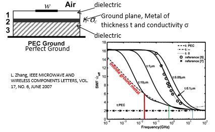
Fig. 5 — Impact of metallization on heat spreader and device performance
A diamond heat spreader is typically metallized with less than 5 mm of gold. Therefore, to isolate the ground plane from the diamond and layers underneath, the operational frequency must exceed 1.5 GHz.
Boron Doped Diamond Heat Spreader
Thermal conductivity of BDD is reduced from undoped CVD diamond values due to increased phonon scattering by substitutional boron. However, the thermal conductivity of boron-doped diamond is still much higher (Fig. 6) than other electrically conductive materials (Cu, CuW, CMC, etc.), and it is higher than other common high thermal conductivity dielectric materials (BeO, AlN). Although boron doping reduces the thermal conductivity of CVD diamond, BDD remains nearly twice as thermally conductive as other common thermal spreaders.
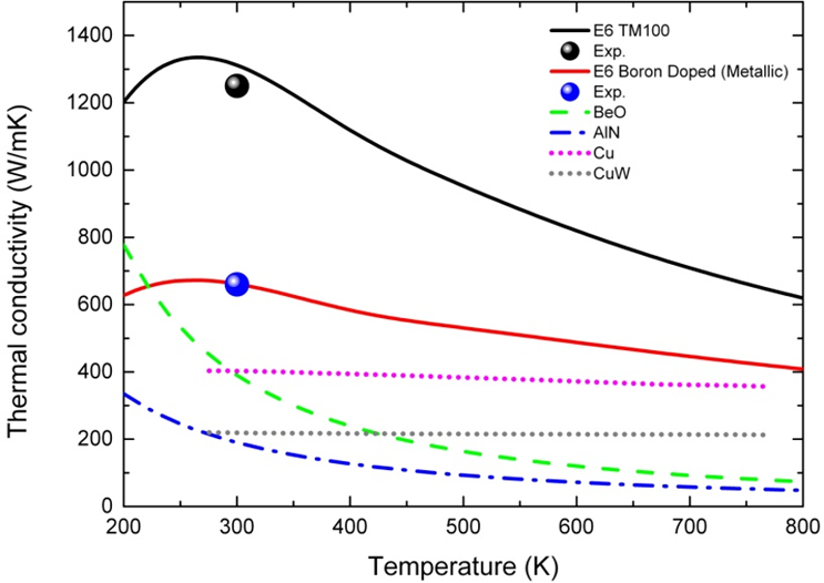
Fig. 6 — Thermal conductivity of various heat spreading materials as a function of temperature (Individual balls represent measured data clusters)
Finite Element Analysis: Impact Of Thermal Heat Spreaders On Junction Temperature
A finite element analysis was used to predict the expected performance of various heat spreaders for a high power GaN device dissipating up to 10 kW/cm2. Fig. 7 depicts the structure when enabled by BDD and presents the temperature profile of the device driven at 10 kW/cm2,
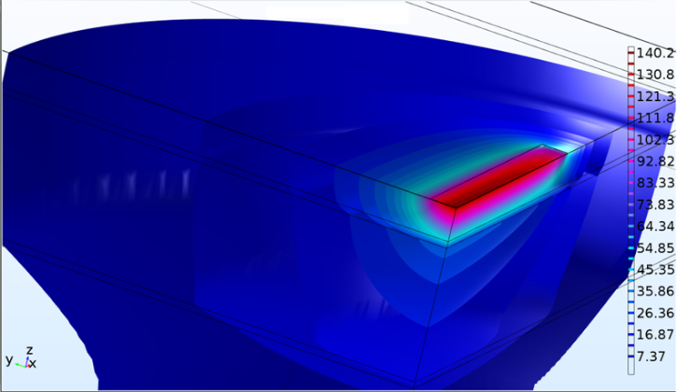
Fig. 7 — Structural details of the simulated high power GaN-on-Si device, mounted on various heat spreader materials (BDD, Cu/W, CMC, Cu, etc.) and bonded to a copper heat sink
The lower thermal resistance of boron-doped diamond resulted in lower overall junction temperature, in a GaN/Si device, by more than a 20 percent, compared to a standard CuW flange (Fig. 8). As heat is the primary enemy of most microelectronic devices, lower junction temperature translates to improved reliability and increase lifetime.
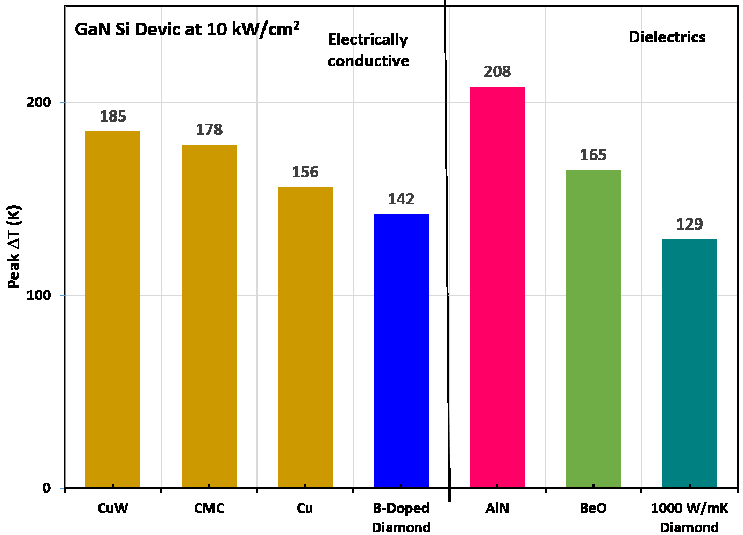
Fig. 8 — Peak junction temperature of GaN/Si HEMT mounted on various heat spreaders.
Boron-Doped Diamond Heat Spreader At Various Frequencies
Using thick BDD with metallic conductivity, instead of common metal/diamond, enables better isolation of the ground plane below 1.5 GHz by increasing the skin depth. The metallic-like heat spreader reduces the slow wave mode and the capacitive coupling between ground planes found in metallised dielectrics below 1.5 GHz. It should be noted that a gold metallization still might be beneficial to reduce the electrical resistance of the BDD substrate.
For electronic applications operating below 1.5 GHz, typical metallized heat spreaders (1000-2000 W/mK) may introduce unwanted couplings between grounds due to capacitive coupling of the metallized ground plane in this frequency range. In this region, it is functionally beneficial to sacrifice some of the ultra-high thermal conductivity of diamond by making it electrically conductive.
Viewed over a wide spectrum of frequencies, BDD shows promise across a range of electronics, from solid state RF PAs and advanced application specific integrated circuits (ASICs), to 5G wireless and phased array radar.
About The Author
Firooz N. Faili is the Principal Application Engineer for Thermal Products at Element Six, focused on developing new and sustaining existing products and markets. He has spent over 25 years on technology development at startups and established companies in semiconductor industry. He co-founded companies focused on developing GaN-on-diamond and novel CVD diamond growth technology. As a Principal Technologist at Varian Semiconductor, he worked on dielectric and conductor etch and CVD development; as Chief Technologist at LASA Industries, he was responsible for the development of a single cluster-tool methodology for multi-level metallization and prototyping of ASICs. He holds a BS and MS in chemical engineering, as well as a Ph.D. in material engineering.
References
[1] R.S. Balmer, J.R. Brandon, S.L. Clewes, et al., “Chemical vapor deposition of synthetic diamond: materials, technology and applications,” Journal of Physics: Condensed Matters, 21(36), (September 2009)
[2] H. Lui and D. Dandy, “Studies on nucleation process in CVD diamond: an overview of recent developments,” Diamond and Related Materials, Volume 4, Issue 10, Pages 1173-1188, (September 1995)
[3] Ken Okano, Hidetoshi Naruki, Yukio Akiba, Tateki Kurosu, Masamori Iida, Yoichi Hirose and Terutaro Nakamura, “Characterization of Boron-Doped Diamond Film,” Japanese Journal of Applied Physics, Volume 28, Page 1066, 1989
[4] B. Rémy, D. Maillet, S. André, “Laser-Flash Diffusivity Measurement of Diamond Films,” International Journal of Thermophysics, Volume 19, Pages 951-959, May 1998
[5] F. Faili, W. Huang, J.A. Calvo, et al., “Disturbed and scattered, the path of thermal conduction through diamond lattice,” ITherm 2016, (May-June 2016)
[6] Thomas Obeloer, Bruce Bolliger, “Application of Diamond Heat Spreaders for the Thermal Management of GaN Devices,” Electronics Cooling, April 14, 2016
[7] Y. Iwashita, “Reduction of RF Power Loss cause by skin effect,” Page 700, Proceedings of LINAC 2004
[8] L. Zhang, IEEE Microwave and Wireless Components Letter, Vol. 17, No. 6, June 2007