
Bluetooth Radio Design Considerations for Cellular Handset Application

Contents
•Introduction
•Core Bluetooth Radio Specifications and Handset Requirements
•Blueooth RX Mode
•Bluetooth TX Mode
•Antenna Isolation
•Antenna Filter
•Marketing Requirements
•Low Cost
•Low Power Consumption
•Small Size
•Time to Market
•W7020 Block Diagram
•Handset Maker Concerns
•Manufacturing Ease
•Radio Vendor Volume Capacity
•Bluetooth Certification
•Summary
Introduction
Bluetooth enabled digital cellular handsets are projected to be among the initial applications for Bluetooth links and the early volume leader for mass production. However, the digital cellular radio is already a rather complex system. Now when the aspect of embedding multiple transmitters and receivers such as Bluetooth and GPS into ever-shrinking mechanical assemblies is considered, the technical challenges are even more severe. All of this is expected to be achieved with minimal degradation to the original cellular handset performance. This will require proper shielding & isolation, filtering, high linearity and rigorous RF-system analysis.
Indeed the cellular handset environment does present the most stringent system requirements on the Bluetooth radio. Performance of the Bluetooth Receiver (RX) Out-of-Band Blocking and Transmitter (TX) Spurious Emissions needs sufficient front-end filtering, yet low insertion loss. The optimal radio solution needs to consider the system requirements, various design implications imposed by the host, and manufacturing yield.
The W7020 Bluetooth Class 2,3 radio subsystem is a complete RF solution in an easy-to-use module. The radio module requires only an external antenna connected through a 50-W characteristic impedance line and a 13 MHz crystal or external reference-clock signal to enable Bluetooth radio communication links. It provides a seamless interface to many available baseband solutions to create a complete Bluetooth node.
Core Bluetooth Radio Specifications and Handset Requirements
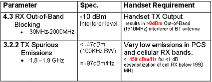
For a radio design to be a fully compliant Bluetooth 1.0B certified solution, obviously the core specifications must be met. However, as Table 1 shows, there is a gap in what the Bluetooth spec. requires and the performance needed within the handset for certain parameters.
Back to top
Bluetooth RX Mode
For the case of a PCS 1900 handset transmitting at +32dBm and the on-board Bluetooth radio receiving, the PCS 1900 signal level would be +2dBm as an Out-of Band Blocker at the Bluetooth antenna, assuming 30dB isolation from the PCS antenna to Bluetooth. The Bluetooth radio front-end filtering must then provide additional rejection over what the core spec. would have required.
Back to top
Bluetooth TX Mode
For the case of Bluetooth transmitting while the PCS handset is receiving, the 2.4GHz Bluetooth TX acts as a blocking signal to the PCS RX, but the level is lower than what the PCS system blocking requirements call for and it is filtered out in the PCS front-end. Bluetooth TX interference is more critical for a GSM handset than for the narrow-band TDMA systems by virtue of the integrated channel power level. The Bluetooth TX power in its 1MHz channel BW is 9dB lower when integrated in the TDMA 30KHz BW, but only 2dB lower for GSM with a 200KHz BW.
However, the worst case scenario for Bluetooth TX interference is its wideband noise that falls into the PCS and cellular RX bands. Table 1 indicates that the noise level should be < -150 dBm/Hz for < 1dB desensitization of the PCS RX:
Starting with thermal noise at the PCS antenna, -174 dBm/Hz + -180 dBm/Hz added noise, results in –173 dBm/Hz or 1 dB degradation of the RX sensitivity.
This requirement is > 50dB harder than what the Bluetooth core spec. calls for. The W7020 output noise is < -160 dBm/Hz and so PCS RX desensitization is < 0.1dB which is far more desirable. This more difficult TX spurious emissions requirement has design implications on the Bluetooth radio VCO loaded Q, the TX noise level, and front-end antenna filtering.
Antenna Isolation
The previously mentioned 30dB isolation from the cellular handset antenna to the Bluetooth antenna is a critical target. The achievable isolation is heavily dependent on the antenna polarity orientation, resonance bandwidth that will give some additional out-of-band filtering, and placement within the phone. The issue is shown in Figure 2.
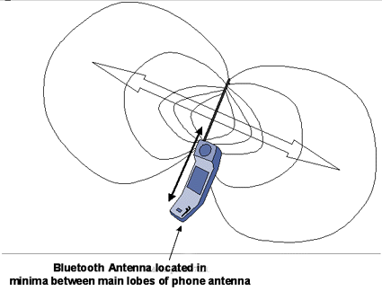
A simplified understanding assumes reciprocity i.e. the loss is the same in both directions between the two antennas. This holds true for the far field condition. However if both antennas are using the same ground plane, it is difficult to determine far field from near field. Currents from both antennas flow through the ground plane and would radiate. This problem can be resolved by using segmented or slotted ground planes or separate grounds.
Back to top
Antenna Filter
The antenna filter then must provide an additional 25 to 35 dB rejection below 1.92 GHz to reduce the Blocker from the handset TX below the input –1dB compression point of the Bluetooth RX. This also allows for lower current consumption in the RX front-end. The filter must also have low insertion loss for best RX sensitivity. Front-end losses prior to the LNA reduce RX sensitivity dB for dB.
The LTCC module allows the filter to be completely embedded in the substrate. The xy area is about the same as an external discrete ceramic filter or effectively smaller due to the multi-layer stack up which LTCC provides, allowing for solder-bumped flip-chip ICs and other surface mount (SMT) components to be reflowed on top of the substrate. Also for the filter, there are no additional Bill-of-Materials (BOM) costs or assembly & handling required.
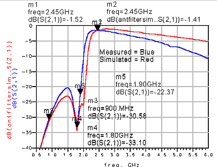
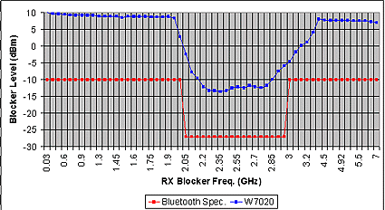
The embedded filter S21 characteristic for the Bluetooth 2.4 to 2.5 GHz ISM passband and rejection for PCS and cellular RX bands is shown in Figure 3 for both simulation and actual measured responses. The W7020 1st pass filter performance exceeded the RX blocking requirements and passed Bluetooth certification. The RX blocking performance is shown in Figure 4. Only minor redesign is necessary to optimize the PCS band rejection. The accuracy of modeling of the embedded passives in the substrate is critical to reducing the number of re-design iterations needed.
Marketing Requirements
There are key marketing requirements for a successful cellular handset product. These transfer directly down to the Bluetooth radio solution. Each of these factors can be evaluated in isolation, but the optimal solution needs to examine the trade-offs or balance of each of these requirements.
Low Cost
Low cost considerations as well as performance advantages start with determining the Bluetooth system partitioning. Initially at the higher level, there is the demarcation of the RF to Baseband (BB) interface. The necessary hardware functions to be implemented between the Bluetooth radio and BB are for the TX path, modulation and gaussian filtering, and for the RX path, demodulation, data slicing, and timing recovery/correlation. The decision comes down to either implementing the functions separately in the most cost-effective IC technology or combining in a single IC & simplifying the interface.
Next the partitioning of the radio functions such as antenna, filtering, TX/RX switch, matching networks, front-end LNA and TX power stages, VCO tank, and synthesizer loop filter between on-chip or off for a given performance requirement must be evaluated. The RFIC should use a cost-effective level of integration. Generally, higher levels of integration lead to cheaper overall solution cost, but a large-die IC becomes less economical as it yields poorly and is more difficult to package. This higher die cost can start to offset the initial savings in external BOM.
Another cost decision is whether to offer a complete solution within a module or to pass on certain functions as the OEM customer's responsibility. These include antenna filtering and other SMT passives.
After working through the system partitioning choices, the next step for low cost consideration is the radio architecture and implementation. Here it is more direct that the goal should be to minimize the external off-chip BOM. RFIC process technology options, BiCMOS, Si Bipolar, SiGe BiCMOS, and RFCMOS present a complex decision matrix for given performance and cost targets.
Packaging is another important factor as cost can vary considerably from system-on-a-chip (SOC) implementation to system-in-a-package (SIP). With SIP, the package becomes an integral part of the system rather than just an interconnect carrier for the IC. For an RF module, the cost effective substrate choice depends on more than just the inherent manufacturing costs of the material, there is also the number of off-chip passives needed, can they be efficiently embedded in substrate, and the resulting substrate size.
Low Power Consumption
The choice of radio architecture along with the IC process technology that it is implemented in primarily determines the solution power consumption. A re-spin of an existing DECT IC has compromises in current & BOM and does not present an optimal solution. The architecture should be optimized to the Bluetooth system standard.
The W7020 RFIC uses a Low-IF RX with integrated active BP filter. The IF is << fT of the IC process so the completely on-chip IF circuits can use a low bias current for a given noise figure. Also the Bluetooth RX in-band interference specs. are tailored to a low-IF scheme with relaxed in-band image frequency and adjacent ±1MHz to the image interference levels.
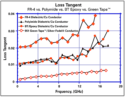
Also important for low power consumption, the W7020 uses low-loss LTCC module substrate technology. This provides high-Q embedded passives and allows for low insertion loss RF front-end functions. For comparison, a 5nH inductor embedded passive in LTCC has Q = 40 @ 2.4 GHz and ±5% tolerance, the typical inductor on an IC without more costly levels of metal has Q < 10 and worse tolerance. As seen in Figure 5, the loss of FR-4 is 10X that of LTCC.
Low cost design choices can result in worse power consumption. For example, although a fully integrated VCO will have less BOM than one using an external tank, but the worse phase noise performance would require more front-end filtering also giving higher insertion loss and the IC will use more bias current to deliver the same power to the antenna. Another example is in using RFCMOS. More bias current in the RX will be required for a given input –1dB compression point.
Small Size
For small size considerations, the RFIC should have a high level of integration to minimize the external off-chip BOM. An RF module substrate with embedded passives like multi-layer thick-film LTCC greatly enables small size for the radio solution. With >50 layers possible, it gives the ability to layout a design in 3-dimensions and then mount RFIC on top. Embedded inductors, capacitors, striplines, and µ-strips provide a suitable tool kit for RF design and good isolation can be obtained between radio sections in close proximity.
The best choice of substrate varies on a case by case basis depending on the number of off-chip SMT passives needed and the complexity level of the radio system. A comparative example is shown in Figure 6. Size and cost of a Bluetooth radio module was determined for 3 different substrate technologies. With LTCC as the benchmark, the module size was 6 X 6 mm, 10-layer design with all front-end functions embedded except for SMT decoupling and synthesizer loop filter caps mounted with the flip-chip RFIC on top of the substrate. The FR-4 (epoxy-E Glass) and Bismalemide trianine (BT) organic laminate substrates were 4-layer designs with SMT inductors and capacitors. Larger number of layers can be used in FR-4 and organic laminates, but then the manufactured material cost starts increasing. Since the LTCC module was about half the size of the others, the module cost came out about the same for all. However the overall BOM is larger for the printed circuit board (PCB) solutions.

Time to Market
For Time to Market (TTM) considerations, the radio architecture development should start with the Bluetooth core RF specs. 1.0B, then flow into defining the proper product specs to meet the system requirements. In this way, the radio architecture complexity can be limited to that needed to meet the system requirements. This controls the risk of various design approaches and technology choices. This methodology was applied in the W7020 development.
The resulting outcome was that the 1st engineering samples were fully functional and the very next design revision of the module combined with a BB IC and flash memory passed Bluetooth certification. The W7020 has also passed certification in OEM customer products.
Back to top
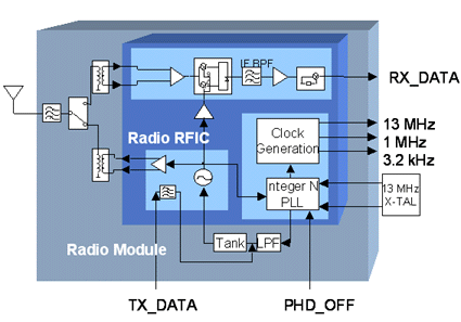
W7020 Block Diagram
The W7020 Bluetooth radio module block diagram is shown in Figure 7. The radio is based on a BiCMOS RFIC. The RX path is completely integrated from LNA to sliced RX Data output including integrated IF bandpass and post-detection filtering. The TX architecture is simple and uses low bias current. The TX Data is guassian filtered and then directly injected onto the off-chip VCO tank which drives the power stage for the TX output. The integer-N synthesizer uses an on-chip 13 MHz reference oscillator that only needs to have a 13MHz crystal applied external to the module or can be overdriven by the GSM handset reference clock. The RFIC provides a buffered reference clock signal for the BB, along with a 1MHz sync clock to the BB for the TX Data timing. A low-power digital 3.2KHz slow clock is provided to the BB to keep system time during sleep mode.
The front-end antenna filter, TX/RX switch, baluns and impedance matching networks are integrated into the LTCC substrate comprising both embedded passive inductors, capacitors and striplines and other assembled SMT components. Since LTCC allows for multi-layer stack-ups with multiple ground planes, the baluns are designed in stripline. This gives much better tolerance performance than Pseudo-balun L-C, C-L designs, which do both matching and phase shifting/combining of the differential signal to single-ended.
The TX output power is 0dBm meeting Bluetooth Class 2 requirements and can tune over the complete Bluetooth 2.4GHz ISM band of 2.400 to 2.497 GHz. The RX sensitivity is typically –78dBm for 0.1% BER and meets all interference and blocking requirements without the need for additional external filtering.
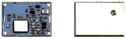
The module size is 9.7 X 14.0 X 1.6 mm and uses Land Grid Array (LGA) solder pads. The advantage of LGA over a Ceramic Ball Grid Array (CBGA) package is that the LGA package can easily shrink in size and not become pad limited for a given I/O.
Back to top
Handset Maker Concerns
There are also the cellular handset maker concerns that play strongly into the requirements for the Bluetooth radio solution.
Back to top
Manufacturing Ease
The W7020 is virtually a "shrink wrapped" System-in-a-Package module. There is no RF-critical design and layout work needed for the host product. To form a Bluetooth node, simply hook up the antenna, dc power and BB interface. The module has all of the RF-critical functions and passives integrated into the LTCC substrate.
This results in a reduced "cost of ownership" for the OEM using the W7020 Bluetooth radio. Thus the handset maker immediately recognizes the advantages of this radio solution through easier development and production including design, PCB layout, testing, certification, inventory and supply chain management, and end-product yield. As opposed to a standard IC packaged RF solution, which requires the OEM to handle and assemble many external SMT passives, packaged active devices and filters as well as take on additional RF PCB design work, the W7020 single-component Bluetooth radio module forms a complete radio.
Radio Vendor Volume Capacity
The handset makers manufacturing strength is linked to its supply chain and so the vendors inherent manufacturing capability and product yield are critical items for everyone's success. The W7020 is designed in proven technologies that are in high volume manufacture within the industry. The RFIC process is BiCMOS and substrate in LTCC. The radio architecture has a low BOM and the RFIC has an optimal level of integration so that it is high yielding. The LTCC substrate technology has very good embedded passives to help form the necessary radio performance.
The radio production test is also critical for shipping performance. It needs to be time efficient since for high volume production, even seconds of test time add significant cost to the product. In contrast, the test needs to be thorough enough to verify RF performance according to the RF core spec. 1.0B.
Back to top
Bluetooth Certification
This is a major milestone for the OEM development process to start into manufacture. The Bluetooth radio takes this into consideration from the very start by the radio architecture development starting with the core RF specs., and the RF product electrical specs. derived through systems analysis.
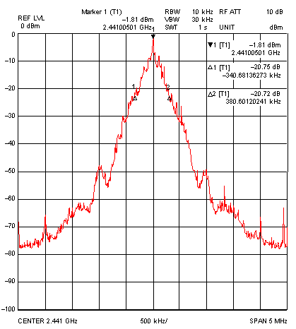
The radio production test also plays an important part in ensuring certification for the handset to the extent that the test verifies the Bluetooth RF test spec. 0.9. For example, the W7020 TX modulation spectrum, shown in Figure 8, –20dB BW test is the same as the FCC requirement that is part of the Bluetooth certification.
The W7020 SIP module has many advantages towards promoting OEM successful certification. As the W7020 is a complete radio with production testing that directly verifies many of the certification performance parameters , it nearly can be "Pre-certified" standalone. It essentially is providing a "known good Bluetooth radio" into the handset.
Summary
In summary of the Bluetooth radio design considerations for the cellular handset application, there is a caution on "low BOM" as the only cost focus. There should be some attention in the development phase to avoiding additional "hidden costs" that come with particular architecture or technology choices that are due to subsequent poor manufacturing yields or delayed product entry into the market.
The "winning" Bluetooth radio designs are those that consider the entire development process in that the architecture satisfies the optimal balance of the discussed Marketing Requirements, and that the design enables high manufacturing yields. It promotes handset maker success by ease of design-in, manufacturing ease, and ease of achieving Bluetooth certification.
For more information contact Agere Systems at 1-800-372 2447, or visit www.agere.com