
Analog Devices Introduces Clock ICs With Sub-Picosecond Jitter Performance

Norwood, MA -- Analog Devices unveiled a series of clock ICs that meet rigorous signal-processing requirements in today's high-performance electronics applications, such as wireless infrastructure transceivers, instrumentation, and broadband infrastructure. Within these applications, signal processing schemes are reaching astounding speeds, and jitter, or the uncertainty of the clock edge, can cause transmission errors and have an adverse effect on a system's overall performance. ADI's new clock ICs feature sub-picosecond jitter performance, which enables the devices to deliver a clean system clock for noise reduction in system-critical signal chains.
In addition to low jitter, ADI's clock ICs improve system performance through the integration of several key functions that eliminate the need for multiple discrete components, reduce board space, and ultimately reduce BOM (bill of materials) costs. These features include a low-phase-noise PLL (phase locked loop) frequency synthesizer core, programmable dividers, and adjustable delay blocks. Combined with sub-picosecond jitter performance, these features make ADI's clock ICs the industry's best at maximizing the performance of critical-signal-path components, such as analog-to-digital converters (ADCs), digital-to-analog converters (DACs), direct digital synthesizers (DDSs), and mixed-signal front end (MxFE) devices.
"As the industry leader in data conversion, ADI continually seeks to provide customers with the highest levels of system performance, and ADI's clock ICs are key to improved system performance," said Kevin Kattmann, product line director, High-Speed Converters, Analog Devices. "As frequencies and data rates move higher and higher, the accuracy of a system and the performance of its converters is increasingly limited by the quality of the clock signal. ADI's new series of clock ICs combines best-in-class signal integrity with innovative functionality, allowing customers to achieve optimum system performance, while greatly simplifying the clock tree design task."
ADI's clock IC offerings include both clock distribution and clock generation devices.
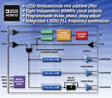
ADI's Clock Distribution ICs -- AD9510, AD9511, and AD9512
ADI's clock distribution IC series includes the AD9510, AD9511, and AD9512. These devices feature sub-picosecond performance over a broad frequency range, higher levels of integration, and more programmability.
Low-phase-noise clock outputs with sub-picosecond jitter
Low phase noise and low jitter are key to reducing overall noise in a signal path. ADI's clock distribution ICs feature LVPECL outputs, as well as user-selectable LVDS and CMOS options:
- LVPECL outputs operate to 800 MHz with additive jitter less than 250 fs (femtoseconds) rms.
- LVDS and CMOS outputs operate up to 800 and 250 MHz, respectively.
- In both LVDS and CMOS modes, the additive jitter is less than 300 fs rms.
The voltage levels for both LVPECL and LVDS clock outputs are programmable, allowing the system designer to determine the best voltage swing for a given application. The AD9510 offers the most flexibility, mixing LVPECL, LVD,S and CMOS logic for a total of eight independent clock outputs. For designs requiring fewer outputs, the AD9511 and AD9512 pack five independent outputs into a smaller package at reduced power consumption.
Programmable dividers
ADI's clock distribution ICs eliminate the extra components required to generate gate delays and phase shifts, by using dividers with dramatically increased functionality. Each clock divider is programmable to any integer ratio from 1 to 32, offering flexibility when handling multiple frequencies on one PCB (printed circuit board). The divide function also includes a user-selectable offset word that enables channel-to-channel phase control. Because the devices perform phase control inside the divider block, they maintain much lower jitter than equivalent discrete implementations.
Programmable delay
ADI's clock distribution ICs feature on-chip programmable delay allowing users to adjust for set-up and hold-time requirements between data converters and digital ASICs, FPGAs (field-programmable gate arrays), and digital up/down-converters, without adding extra clock hardware. All three AD951x products include at least one fine-delay-adjust channel with a programmable full-scale range from 1 ns to 10 ns. A 6-bit delay word offers 64 unique delay settings with step sizes as low as 16 ps.
Integrated PLL frequency synthesizer core
Both the AD9510 and the AD9511 integrate a low-phase-noise, 1.5 GHz PLL frequency synthesizer core on chip. The PLL is optimized for clock applications and consists of a programmable reference divider, a low-noise phase frequency detector, a precision charge pump, and a programmable feedback divider. For applications that do not require an on-chip PLL, the AD9512 offers two 1.5 GHz clock inputs and five independent clock outputs.
Source: Analog Devices