
A Fully-Integrated 3.5GHz Single Chip GaN Doherty PA For sub-6GHz 5G
By Robert Smith, Stuart Glynn, Jake Greene, and Liam Devlin, Plextek RFI

5G roll-out will take place in two distinct frequency ranges — the sub-6 GHz region (FR1) and the mmWave frequencies (FR2). The 5G networks operating at mmWave frequencies promise very high data rates across small network cells (picocells), typically in densely populated cities. However, it is expected that the first 5G networks will utilise sub-6 GHz frequencies and comprise large cells in cities, towns, and rural areas.
The use of the sub-6 GHz bands will make the transition from 4G/LTE to 5G easier for service providers (whose existing LTE/4G networks already use channels within bands between 600 MHz and 3.5 GHz) and will retain the benefit of superior long-distance propagation characteristics available at lower frequencies. As with current 4G/LTE networks, the sub-6 GHz 5G base stations will transmit high-power RF signals over large areas, or “macrocells,” each requiring a high-efficiency linear power amplifier (PA) to avoid unnecessary power consumption during transmission. One of the expected sub-6 GHz 5G bands will be between 3.4 GHz and 3.8 GHz.
Many conventional GaN PAs are designed to operate in Class AB, which can provide very good power-added efficiency (PAE) at compression. However, when backed off to improve linearity, PAE drops off rapidly. Use of Doherty amplifier topology allows for significant improvements in PAE when operated at back-off from compression. A good summary of the various implementations of the Doherty amplifier can be found in [1].
This article describes an S-band, packaged Doherty PA MMIC for use in 5G base station transmitter applications. The design was realized on GCS’ 0.4 μm Gallium Nitride (GaN) process and assembled by Filtronic into an 8 mm x 8 mm custom laminate QFN-36 package.
The PA delivers 45 dBm of peak (saturated) RF power from a 28 V supply rail, with a peak PAE of 50 percent and a PAE of 31.5 percent when operating at 8 dB back-off. It spans 3.4 GHz to 3.8 GHz, and includes the allocated international 5G channels in this band. The design, simulation, assembly, and subsequent measurement of the power amplifier IC are described.
Doherty Amplifier Basics
5G communications will use modulation schemes with high peak-to-average power ratios (PAPR). Since the PA in the transmitter is required to amplify large but infrequent peaks in signal amplitude, it spends most of its conduction time amplifying comparatively small signals, and thus draws excess current from the power supply between peaks.
While a conventional Class A amplifier could provide the required linearity, it would be too inefficient. Better efficiency could be offered by Class D/E/F amplifiers, but with the consequence of degraded linearity. Class AB or Class B power amplifiers often are used as a compromise between efficiency and linearity, but these may only provide a typical backed-off PAE of 10 to 15 percent.
The Doherty topology employs two amplifiers: the ‘main’ and ‘auxiliary’ amplifiers (sometimes referred to as ‘carrier’ and ‘peaking’ amplifiers, respectively). The main amplifier is biased in Class AB, while the auxiliary amplifier uses a Class C bias. The basic idea is that only the main amplifier is operating when the RF signal levels are small but, as the input drive starts to rise, the auxiliary amplifier also conducts. Thus, both amplifiers are conducting under large-signal drive, but only the main amplifier is in use at back-off.
A block diagram of the Doherty amplifier used in this development is shown in Fig. 1. The output matching network consists of two impedance transformers, which ensure that optimal impedances are presented to the amplifier in both compressed and backed-off operation. By operating at two input power-dependent bias points, this topology allows the amplification of both small and large-signal inputs without compromising efficiency.
The impedance inverter at the output of the main amplifier results in a 90-degree phase shift between the main and auxiliary amplifiers. To ensure the main and auxiliary output powers are combined in large-signal operation, a corresponding 90-degree phase shift has to be added to the input of the auxiliary amplifier branch.
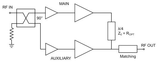
Fig. 1 — Block Diagram of the Doherty MMIC Power Amplifier
Fig. 2 compares the theoretical efficiency versus output power of an ideal Doherty amplifier (blue) to a Class B amplifier (red). The efficiency at saturation is 78.5 percent in both cases, but the Doherty PA also achieves this efficiency at 6 dB back-off. This efficiency curve has been plotted using ideal analysis and does not account for knee voltage and other realistic transistor effects. In a classic Doherty design, the two efficiency peaks are spaced 6 dB apart; however, it is possible to modify this spacing by changing the auxiliary amplifier’s bias point, or by adopting an asymmetrical design.
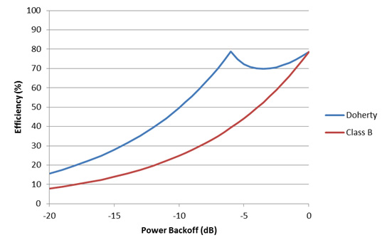
Fig. 2 — Theoretical Efficiency vs Output Power of a Doherty Amplifier compared to a Class B Amplifier
MMIC Design
The Doherty PA was developed on GCS’ 0.4 μm GaN-on-SiC process. A block diagram schematic of the MMIC can be seen in Fig. 1. An identical design was used for the main and auxiliary amplifiers, commonly referred to as the ‘symmetrical’ Doherty configuration. It should be noted that a practical symmetrical Doherty amplifier (termed ‘Doherty Lite’ by Cripps [2]) does not exhibit the ‘twin peak’ response shown in Fig. 2, but still show a substantial efficiency improvement at back-off compared to the conventional Class B amplifier.
An asymmetrical Doherty amplifier would use an auxiliary amplifier capable of higher peak power than the main amplifier. This approach has an optimum efficiency at a higher level of back-off than the symmetrical design. It has been shown, however, that improved back-off efficiencies can be realized using the symmetrical configuration, which also has the advantage of a simpler design and better power utilisation factor (PUF) [3] [4].
The output stage of each two-stage amplifier block consists of two parallel transistors, both driven by a single, smaller device. The transistor drive ratio between the first and second stages is carefully selected to provide sufficient linear power to the output stages without compromising efficiency.
Extensive load-pull simulations at various bias points were performed using GCS’ nonlinear device models. This allowed the optimal device sizes, load impedances, and current densities to be selected for Class AB operation, before synthesis of any matching networks took place.
The driver and output devices were stabilised using interdigitated or serpentine thin-film resistors at their inputs, which enabled low-value resistances to be realized within a compact layout area. The output stage transistor drains were interlinked with a resistor to suppress odd-mode oscillations.
To flatten the transistors’ inherent negative gain-versus-frequency slope, a passive equaliser network was included at the input. The driver stage’s gate bias inductor was implemented in a thin, low-Q metal layer for additional gain-shaping. A lumped-element 3 dB hybrid was used to realise the equal power division and quadrature phase shift at the auxiliary amplifier input.
The Doherty Output Matching Network (OMN) consists of an impedance transformer — used to transform 50 Ω to ROPT/2 — and an impedance inverter, which, in conjunction with the auxiliary PA, performs the power-dependent impedance transformation. The network also incorporates the main and auxiliary output stages’ drain bias networks. When designing the OMN, care must be taken to ensure the auxiliary amplifier is not ‘loading’ the main amplifier in low-power mode.
The MMIC includes on-chip supply decoupling to ensure unconditional stability down to low frequencies. Separate gate bias connections allow the possibility of bias tuning of the fabricated amplifier. The two output stage VDD (drain) supplies are DC coupled, whereas the driver stage drains are independent. The MMIC is designed, however, to draw all drain currents from a single 28 V supply. Ground-signal-ground (GSG) pads were included at the RF input and output to allow RF on-wafer probe testing, if required.
Input Splitter and Driver Stage Design
For a two-stage Doherty design, the driver stage can either be implemented as a single transistor located before the input splitter, or as separate drivers for the main and auxiliary amplifiers. It has been shown [5] that using separate drivers for the main and auxiliary amplifiers, with the input splitter placed before the driver amplifiers, is best for overall PA efficiency.
While most Doherty papers focus on the design of the output impedance inverter, it also is important to optimize the input splitter design. Excess loss in the input splitter will degrade gain (and thus PAE), and an incorrect phase shift at the input will result in imperfect signal recombination at the PA output.
For this design, a lumped-element implementation was used, and steps were taken to ensure a 90-degree phase shift was achieved across the full operating band (Fig. 3). It also is necessary to achieve good isolation between the main and auxiliary amplifier inputs so the auxiliary amplifier’s turn-on point is not affected by the main amplifier. The input splitter’s simulated isolation is shown in Fig. 4.
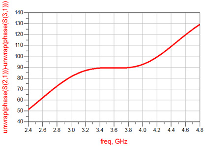
Fig. 3 — Phase Shift of the Input Splitter
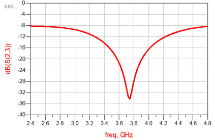
Fig. 4 — Isolation between Main and Auxiliary Inputs
All simulations were performed using Keysight ADS 2017. All of the passive structures were EM-simulated in Keysight Momentum, and the transistor cells were simulated using GCS’ nonlinear device models.
By biasing the main and auxiliary amplifier equally, the MMIC can be operated in a ‘balanced mode’ to provide a comparison between this and the Doherty mode of operation. It should be noted that this balanced mode is not the same as a true balanced amplifier, which includes a quadrature splitter or hybrid at both input and output. All drain supplies are held at 28 V.
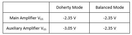
Table 1 — Bias voltages for Doherty and Balanced modes
Fig. 5 shows a plot of the simulated S-Parameters in Doherty mode. Between 3.4 GHz and 3.8 GHz, S21 is > 19 dB and return losses are > 12 dB. The amplifier is unconditionally stable in both Doherty and Balanced modes.
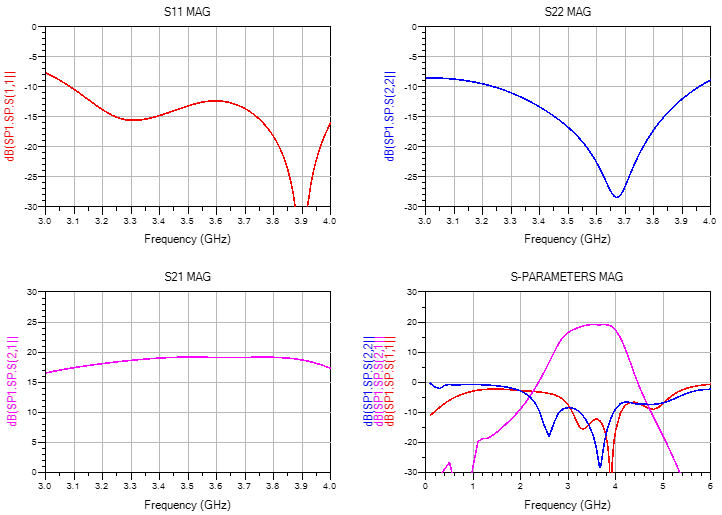
Fig. 5 — Simulated S-Parameters of the Doherty Amplifier
Fabrication, Packaging and PCB Development
A custom laminate SMT package was designed to accommodate the PA MMIC (Fig. 6). This was an 8mm x 8mm QFN-36, which was fabricated and assembled in the UK by Filtronic.
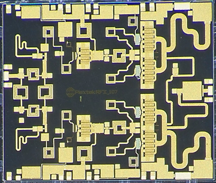
Fig. 6 — The S-Band Doherty PA MMIC (RF input to the left and RF output to the right)
An evaluation PCB was designed to allow evaluation of the packaged part (Fig. 7).
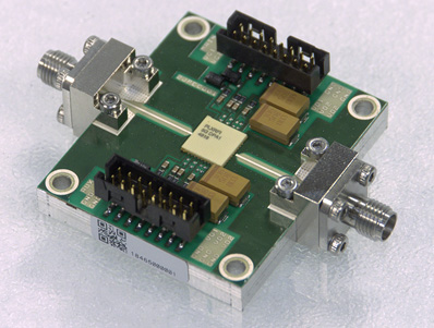
Fig. 7 — The packaged PA assembled onto an evaluation PCB
The evaluation PCB was fabricated on 8-mil Rogers RO4003B on an aluminum baseplate. As well as improving the mechanical stability of the PCB, the baseplate is crucial to the thermal management of the MMIC.
Measured Performance of the MMIC
S-Parameter Measurements
A TRL calibration PCB was designed to allow the measured performance to be referenced to the ports of the package. All measured performance presented here is for the packaged PA assembled onto the evaluation PCB.
Measuring the PA in balanced mode also shows how the auxiliary amplifier’s bias can be tuned for a specific application. If more gain is required, the quiescent bias can be increased, but at the possible expense of PAE at back-off.
Fig. 8 shows a plot of the measured s-parameters (blue traces) compared with the original simulated performance (red traces) for the PA in Doherty mode. Good agreement between simulated and measured is evident.
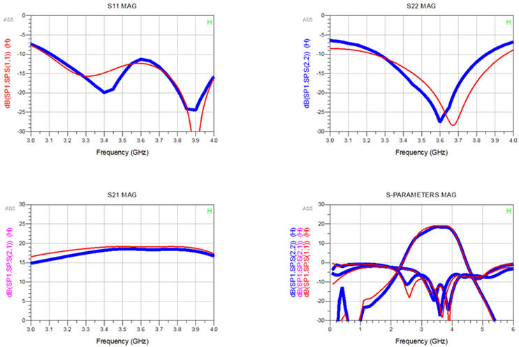
Fig. 8 — Measured (blue) vs. Simulated (red) S-Parameters of PA in Doherty Mode
Large-Signal Pulsed Measurements
When operating at its maximum output power capability, the PA is not designed to be operated under CW conditions. Pulsed measurements were made to demonstrate the PA’s peak power performance, using a 100 µs pulse width at 10 percent duty cycle.
Fig. 9 plots the measured PAE versus output power. The two traces compare the performance in Doherty mode with the performance in balanced mode; the Doherty design PA exhibits significantly better PAE at back-off.
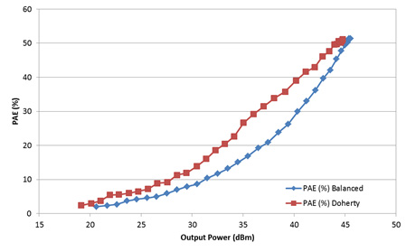
Fig. 9 — PAE vs. Output Power for a 100 µs, 10 percent duty cycle pulsed signal at 3.5 GHz
The measured gain is plotted in Fig. 10 against RF output power for both balanced and Doherty modes. The sharper roll-off of gain in balanced mode is evident.
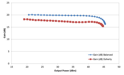
Fig. 10 — Gain vs. Output Power for a 100µs, 10 percent duty cycle pulsed signal at 3.5GHz
Measured PAE versus output power for the Doherty mode PA, across a range of frequencies (3.4GHz to 3.8GHz), is plotted in Fig. 11. The performance is similar at the different operating frequencies.
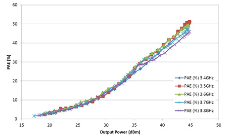
Fig. 11 — PAE vs. Output Power for a 100 µs, 10 percent duty cycle pulsed signal between 3.4 GHz and 3.8 GHz
5G NR Modulated Measurements
Measurements also were made using representative 5G modulated signals. A 100 MHz bandwidth 5G New Radio (5G NR) signal was used for this purpose. While it is unlikely that a 100 MHz bandwidth signal will be used at 3.5 GHz, it could be that 5 x 20 MHz signals could be aggregated in an FDD system. This provides a challenging scenario with which to test the Doherty PA’s linearity performance.
The modulated signal was generated by a Rohde and Schwarz SMBV100B, followed by a pre-amplifier. This pre-amplifier’s effect is included in the modulated measurements, meaning the linearity of the Doherty PA, by itself, actually is slightly better than the figures reported. It also should be noted that no digital pre-distortion (DPD) was used, and this would offer an opportunity for further improvements in linearity.
The measured ACLR (Adjacent Channel Leakage Ratio) is plotted against output power in Fig. 12. Traces for the adjacent channel (ACLR 1) and the adjacent channel but one (ACLR 2) on either side of the transmission channel are plotted. At 8 dB back-off (~ 37 dBm out) this is < -31 dBc for ACLR 1 and <‑41 dBc for ACLR 2.
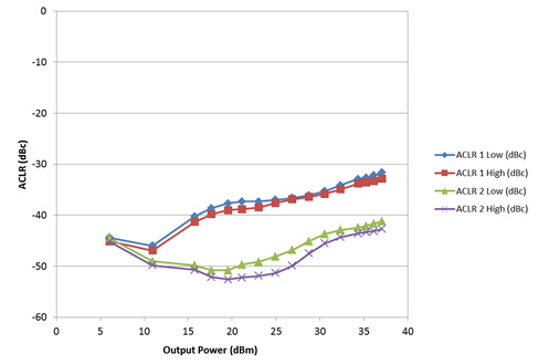
Fig. 12 — ACLR vs Output Power (100 MHz 5G NR Signal) 3.5 GHz, Doherty Mode
Conclusions
The design and evaluation of a fully-integrated Doherty PA MMIC has been described. It has been packaged in a laminate QFN SMT package and measured on a representative evaluation PCB. Performance has been summarised in Table 2. This is achieved in a compact, fully-integrated design requiring only low-frequency decoupling components on the PCB. First-pass design success was achieved due to careful EM-simulation of the matching networks and accurate PDK transistor models, which is evident in the good agreement between measured and modeled performance. Both good back-off efficiency and good linearity were demonstrated with challenging 5G NR signals, and further improvement in linearity would be expected with the use of DPD.
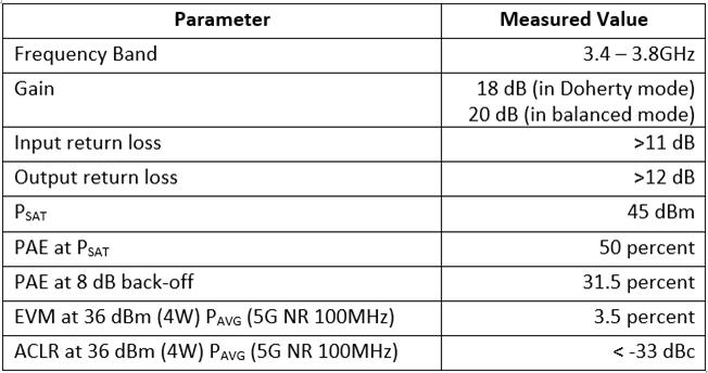
Table 2 — Performance Summary of the Doherty PA
Editor's Note: Robert Smith presented a paper covering this design at a conference the week of April 2, 2019. A video of that presentation is available here.
About The Authors
Robert Smith is a Consultant Engineer at Plextek RFI, where he designs high-performance GaN power amplifiers and millimetre-wave MMICs for 5G applications. He previously worked for Thales in the Netherlands, where he designed transmitter modules for active phased array radar. Robert received his PhD in microwave engineering from Cardiff University in 2013.
Liam Devlin is the CEO of Plextek RFI, a UK-based design house specialising in the design and development of RFICs, MMICs, and microwave/mmWave modules. He has led the design and development of over 90 custom ICs on a range of GaAs, GaN, and Si processes at frequencies from baseband to 90 GHz, and has also developed microwave and mmWave sub-systems using a variety of technologies. Liam previously worked as Chief Designer for Marconi Caswell and was employed by Philips Research Laboratories. Liam has a BEng in Electrical and Electronic Engineering from the University of Leeds, UK.
References
[1] V. Camarchia, M. Pirola, R. Quaglia, S. Jee, Y. Cho and B. Kim, “The Doherty Power Amplifier: Review of Recent Solutions and Trends,” IEEE Transactions on Microwave Theory and Techniques, pp. 559-571, February 2015.
[2] S. Cripps, Advanced Techniques in RF Power Amplifier Design, Norwood, MA: Artech House, 2002.
[3] M. Ozen and C. Fager, “Symmetrical Doherty Amplifier with High Efficiency over Large Output Power Dynamic Range,” 2014.
[4] S. Cripps, RF Power Amplifiers for Wireless Communications, 2nd ed., Norwood, MA: Artech House, 2006.
[5] R. Quaglia, V. Camarchia, T. Jiang, M. Pirola, S. D. Guerrieri and B. Loran, “K-Band GaAs MMIC Doherty Power Amplifier for Microwave Radio With Optimized Driver,” IEEE Transactions on Microwave Theory and Techniques, pp. 2518-2525, 2014.