
A Comprehensive Guide To Active Antennas (Or, "Beamforming 101")
By David Corman, Anokiwave

(Editor's note: This guest column references the coming arrival of 5G technology. Obviously, 5G has arrived and we're already looking forward to 6G. That said, the author's thoughts about active antenna basis, beamforming principles and considerations, and array directivity and gain remain as valid today as they were the day they were written. If you are looking for additional information about beamforming check out this white paper about the effects of mobility on mmWave beamforming in dynamic, urban environments. And if you want to know more about antenna technology this article about future trends in radar and antenna technology is a good start.)
Experts and major industry bodies have spoken — 5G will arrive faster than many envisioned, and our industry is in the middle of an age of innovation that has not been seen for 25 years. Companies developing systems for millimeter-wave (mmWave) 5G networks are in front of regulating bodies, working to anticipate where the market will move and how to meet the needs of their customers. One thing is certain — active antenna beamforming at mmWave bands is an essential technology required to realize the revolutionary new features and capabilities promised by 5G.
This article discusses the basic active antenna beamforming concepts that form the heart of the mmWave 5G system, as well as the general beamforming architectures used in active antennas.
Active Antenna Basics
An active antenna, also known as a phased array antenna, is defined by the Phased Array Antenna Handbook as consisting “of multiple stationary elements, which are fed coherently and use variable phase or time delay control at each element to scan a beam to given angles in space.” Thus, active antennas have electronically-steered beams with no moving parts; steering occurs within the ICs placed at the radiating elements in the antenna.
Active antennas with beamforming ICs have what is referred to as a “soft failure mechanism,” meaning that, because there are many elements in an array, the failure of a few elements typically has little effect on the performance of the antenna as a whole. Active antennas can steer beams in microseconds, as well as support multiple, simultaneous, independently-steerable beams. With no mechanically gimbaled parts, they are low-profile and reliable. Active antennas are able to steer nulls and, since they have many elements, they have high degrees of freedom to block interferers and jammers. Active antennas are capable of generate precise, radiating aperture patterns.
For 5G communications, the antennas will operate at mmWave frequencies, such as 24 GHz, 26 GHz, 28 GHz, 37 GHz, and 39 GHz. At these high frequencies, the wavelengths are very short, allowing many antenna elements to be placed in a compact, highly directive aperture, which offsets the high path loss at mmWave frequencies. Another key benefit of the highly directive beams is that they provide spatial diversity, where multiple beams can reuse the same frequency spectrum, greatly increasing system capacity.
Beamforming Principles And Considerations
The analysis of beamforming by an active antenna is basically an exercise in complex arithmetic. As shown in Fig. 1, we have a linear array along the x-axis, with the antenna elements spaced by d, which is equal to a free-space wavelength divided by two. If each element is energized by the appropriate phase, then a beam can be formed coherently in the far field at the desired direction.
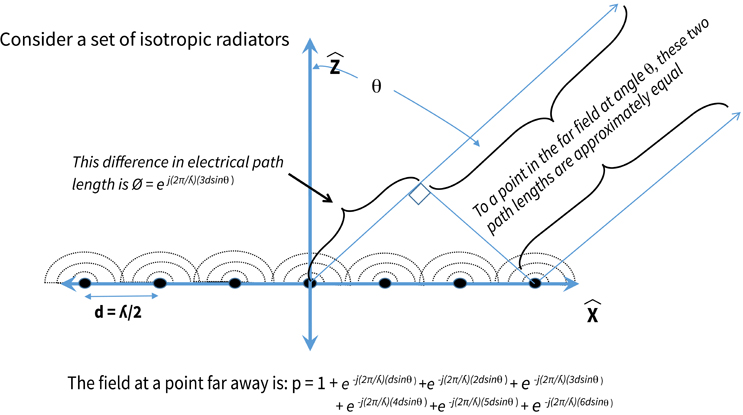
Fig. 1
In Fig. 2, we take an example of an aircraft target that is not in the boresight direction of the array, such that the range from the aircraft to each element in the array is slightly different. The fact that the elements are spaced at d apart, and the angle of arrival of energy from the aircraft is Ɵ, then the incremental path length difference between adjacent elements is d*cos(Ɵ). To compensate for this difference in path length, we can place phase shifters behind each element. When the appropriate phase shift is applied, we can coherently form a beam in the far field. Remember that, to form a beam, energy must arrive at the summation node at the same phase, at the same amplitude, and at the same time. We call this “coherent combining.”
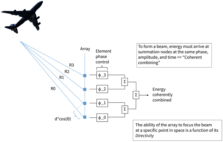
Fig. 2 — Coherent Summation of Energy - Linear Array
Array Directivity And Gain
Directivity is the measure of how concentrated the antenna gain is in a given direction relative to an isotropic radiator. It follows a 10*log(N) relationship, where N is the number of elements in the array. Gain, however, takes into account directivity as well as ohmic and scan losses.
So, in general, array gain equals 10*log(N), plus the embedded element gain (Ge), minus the ohmic and scan losses: Array gain = 10*log(N) + Ge – LOHMIC – LSCAN
Ge is the embedded element gain, which is the gain of a single radiator embedded in the array. If the radiating elements are spaced λ/2 apart in both the azimuth and elevation directions, then the area of each element is λ2/4. Since antenna gain is 4π/λ2*Ae, where Ae is the effective area of the antenna, then the Ge equals π or 5 dBi.
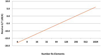
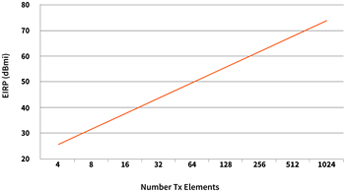
Note that for every element added to an array, the G/T of a receiver (Rx) array increases by 10*log(N). You are increasing aperture size, but the noise figure stays constant. In contrast, the equivalent isotropically radiated power (EIRP) of the transmitter (Tx) array increases by 20*log(N), since for every element you add, you add array gain and transmit power in the far field. It is clear, then, that G/T is much more challenging to achieve with an active antenna than EIRP.
Fig. 3A shows how G/T varies with array size. In this plot, the assumed lattice spacing is λ/2, the system noise figure is 5 dB, and 0.5 dB of loss has been included for both feed loss and radome loss. Fig. 3B shows how EIRP varies with antenna size and RF power/element. In this graph, the same λ/2 lattice spacing is used, and +9 dBm transmit power per element is assumed.
 |
 |
| Fig. 3A — Example: G/T vs. Number of Elements | Fig. 3B — Example: EIRP vs. Number of Elements |
System engineers typically generate detailed G/T and EIRP budgets that take into account a wide range of variables, including system noise figure, embedded element gain, frequency of operation, transmit power per element, loss between the element and the T/R functions, scan loss, the effect of polarizers and radomes, and temperature.
Fig. 4 shows some examples of linear arrays — specifically 16, 32, and 64 elements. The graph shows main lobes and side lobes. The antenna directivity follows 10*log(N), as we’ve established previously, where N is the number of elements in the array. Every time we double the size of the antenna, the beam width halves. And, every time we double the size of the antenna, the directivity doubles, or increases by 3 dBi.
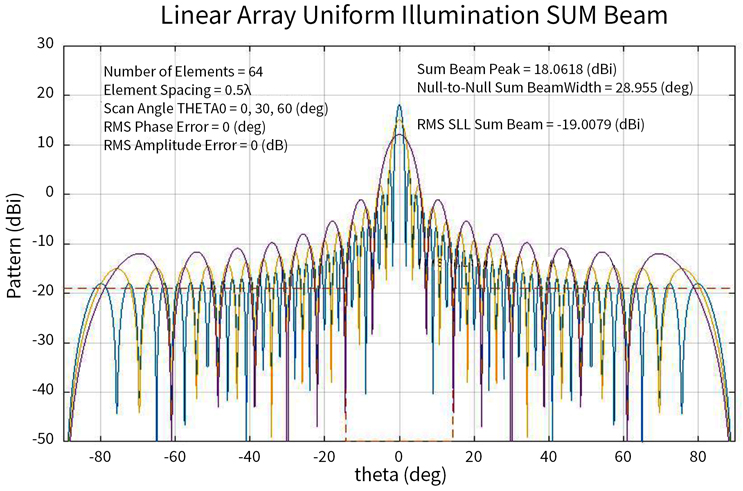
Fig. 4 — Examples of Uniformly Illuminated Linear Arrays: 64, 32, 16 Elements
One characteristic of using phase shifters to steer active antenna beams is called beam squint (Fig. 6). Phase shifters electrically steer a beam by approximating time delay. The result is that they only steer the beam perfectly at the center frequency; they understeer at the maximum operating frequency, and they oversteer at the minimum operating frequency. Yet, phase shifters are preferred over time delay functions because of the tradeoff between accuracy and circuit size. In fact, phase shifters provide good accuracy for almost all active antenna applications, with the exceptions being very wide instantaneous bandwidth applications, such as EW, or very large arrays.
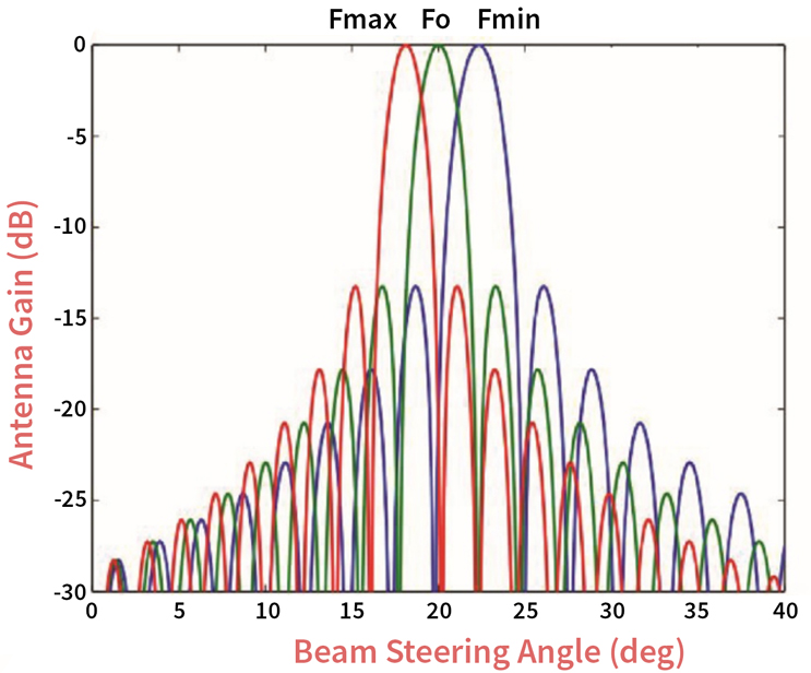
Fig. 5 — Beam Squint
Another characteristic of all active antennas is the loss of aperture gain as the beam is steered away from the boresight direction — defined as Ɵ=0. This characteristic, called scan loss, follows 10*log(cosN(Ɵ)) power, where Ɵ is the scan angle off boresight and N is a numeric value, typically in the 1.3 range, which accounts for the non-ideal isotropic behavior of the embedded element gain.
Fig. 6 plots scan loss in dB vs. scan angle, measured in degrees. Note, at the origin, where the boresight angle is zero, there is no scan loss. As the scan angle is increased to 45 degrees, there is 2 dB scan loss. If you increase scan angle to a practical limit of 60 degrees, there is 4 dB scan loss. Active antennas must therefore be oversized to provide the required G/T and EIRP under maximum scan conditions.
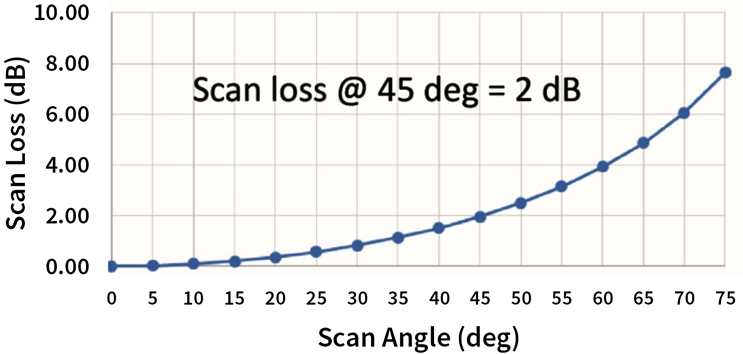
Fig. 6 — Scan Loss
Tapering is the process of assigning different gains to the various elements within the array, where the center elements are assigned the highest gains, and the outer elements are assigned lower gains. Fig. 7 illustrates how various levels of taper can be achieved. The example shown is a 64-element array, so that the maximum gain of each curve occurs at element 32, which is the center of the array. Note that, the more quickly element gain is reduced as the elements get farther from the center of the array, the greater the suppression of side lobes. The graph shows us the effect of side lobe levels of -20, -30, -40, and -50 dB.
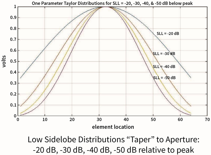
Fig. 7 — Tapering vs. Side Lobe Level
This is why beam forming typically includes amplitude control per element, not just phase control. If all elements are treated with the same gain, it is called “uniform illumination.” Uniform illumination results in -13 dBc first side lobe levels, which may be unacceptable for some applications due to regulatory, interference, or stealth reasons.
Gain control allows the system engineer to adjust the gain per element to achieve the desired lower side lobe levels.
Fig. 8 shows superimposed side lobe levels for various amounts of applied taper — specifically -20, -30, -40, and -50 dB, relative to the peak. Observe the side lobe level suppression, caused by the applied taper. This is a 64-element array with a directivity of 18 dBi (10*log(64)).
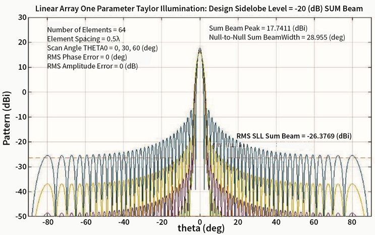
Fig. 8: Sample Taylor Distributions: -20 dB, -30 dB, -40 dB, -50 dB Relative to Peak
At Anokiwave, we typically provide gain controls at the element in the 0–31.5 dB range, in 0.5 dB steps, which is generally sufficient to provide for amplitude taper and other host system control needs. A final note is that taper does not change with scan angle.
Taper can be a good thing, but it does come at a price. When taper is applied, the directivity is less than uniform illumination for the same size array, and the beam widths are broader. Table 1 shows a range of different tapers applied to the array. The top row is the uniform illumination with -13 dBc side lobes, as previously described. Shown below are rows for -20, -30, -40, and -50 dB side lobe levels. Note that their directivity is decreasing, and the efficiency is decreasing. As shown in the table, if a -50 dB taper is applied, a full 2 dB efficiency is lost on the array.
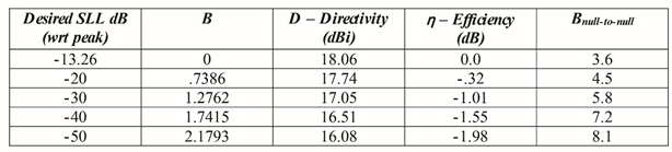
Table 1 — Values of B for desired sidelobe levels in One Parameter Taylor Distributions
Another characteristic of active antennas is grating lobes, which are primarily affected by lattice spacing — the spacing between elements (variable d). To avoid parasitic grating lobes, which are antenna responses in undesired beam directions, the lattice spacing must follow these rules:
- d/λo < 1/(1+sinƟ) for a rectangular lattice (Min. spacing = 0.5 λo at 90 deg scan)
- d/λo < 1.15/(1+sinƟ) for a triangular lattice (Min. spacing = 0.575 λo at 90 deg scan)
Where λo is the free space wavelength, Ɵ is the max scan angle, and d is the spacing between antenna elements. A common value of lattice spacing for active antennas with rectangular lattices is 0.55 lambda.
Fig. 9 shows that required lattice spacing is a function of frequency. The graph plots lattice spacing in millimeters vs. frequency of operation. Note that, for lower frequencies, large lattice spacing makes planar active antennas not very challenging. But look what happens at 28 GHz and above: the lattice is rapidly contracting, which leaves very little room for the T/R functions and beam-forming electronics to fit with the lattice. Fitting within the lattice is critical to high-performance active antennas, as it guarantees minimum feed loss, which maximizes EIRP and minimizes receiver NF.
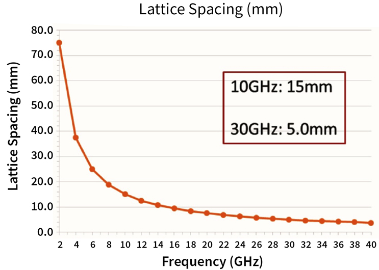
Fig. 9 — Lattice Spacing Example Calculation
λ/2 lattices at 5G mmWave bands are quite small: 5.4 mm at 28 GHz, and 3.85 mm at 39 GHz. This is where the high level of integration with silicon is critical. As mentioned above, the most efficient method to implement planar active antennas at mmWave is to fit the electronics within the lattice using highly integrated silicon ASICs, in the same plane as the radiating elements. As shown in Fig. 10 below, a four-element IC is optimal for signal routing and other component integration.
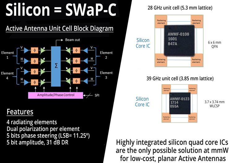
Fig. 10 — Highly Integrated Silicon ICs are Critical to mmW Planar Active Antennas
Active Antenna Beamforming Considerations
Three general beamforming architectures are used in active antennas: analog beamforming, digital beamforming, and hybrid beamforming. In this section, we will describe each approach from a high level and then compare the pros and cons of each approach. Note that, in the sections below the block diagrams all denote receiver diagrams, but transmitter block diagrams look similar, just reversed in direction and using DACs instead of ADCs.
Analog Beamforming
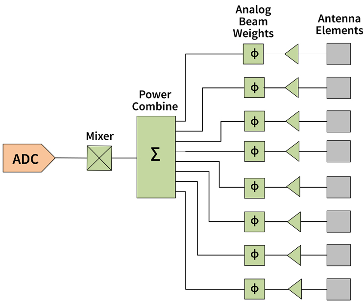
Fig. 11 — Analog Beamforming Block Diagram
All discussion thus far has addressed analog beamforming, where a phase shift is applied to each element in the array followed by coherent power summation. Included in the diagram (Fig. 11) is a suitable frequency downconverter and ADC to complete the system.
|
Analog Beamforming Advantages |
Disadvantages |
|
Simplest hardware implementation |
Single beam |
|
Hardware can fit within the lattice at high frequencies |
Number of beams is fixed by hardware and cannot be changed |
|
Beam benefits from the full array gain |
|
|
Lowest system DC power
|
|
Digital Beamforming
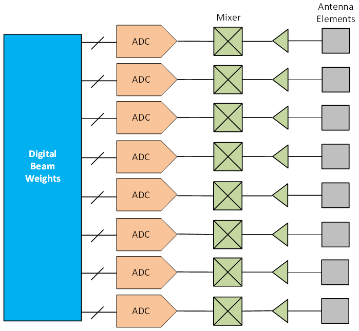
Fig. 12 — Digital Beamforming Block Diagram
In digital beamforming, the beams are formed using complex digital weights, rather than with analog phase shifters. To do this, a full receiver chain from antenna element to digits is required at every element in the array. This is practical only at low frequencies, such as S-band, where the lattices are large and there is plenty of room to place the required hardware on the array. This approach is not practical at mmWave frequencies, since inadequate real estate exists with the tight lattices.
Other significant challenges include high DC power consumption — especially if large bandwidths are to be digitized — signal routing complexity, where multiple bits of I and Q lines must be routed off the array to the digital processor (imagine routing 8 bits of I and 8 bits of Q times the number of elements in the array!), and LO signal routing within the array. On the plus side, if these challenges can be addressed, then this architecture is the most flexible, since multiple beams and nulls can be formed dynamically, with no change in hardware required, and each beam benefits from the gain of the full array.
|
Digital Beamforming Advantages |
Disadvantages |
|
Extreme flexibility with number of beams and nulls |
Highest DC power |
|
Can provide high number of beams |
I/Q signal routing complexity |
|
Number of beams can be changed dynamically with no change in hardware |
LO signal routing complexity |
|
Each beam benefits from the full array gain |
Highest hardware complexity – full RF chain per element in the array |
|
|
Hardware cannot fit the lattice at high frequencies |
Hybrid Beamforming

Fig. 13 — Receive Hybrid Beamforming Block Diagram
Hybrid beamforming is a cross between analog and digital beamforming. The beam concept (Fig. 13) involves the formation of analog (sub-array) beams from a portion of the full array. In Fig. 14, the wide black beam represents the embedded element’s gain, the red beam is the analog sub array beam, and the two blue beams are the digital beams. Only two digital beams are shown for simplicity but, in fact, many beams can be formed.
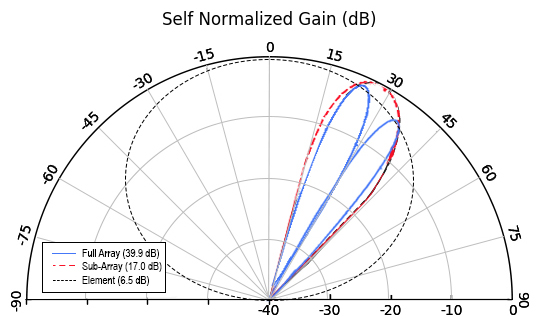
Fig. 14 — Hybrid Beamforming Beam Illustration
The full array is broken into sub-arrays, with an individually steerable analog beam assigned to each sub-array. Then, digital beamforming is used to form many beams within the analog beams. The beauty of this approach is that it can be used at mmWave frequencies, it provides the digital flexibility to dynamically form many beams and nulls with no change in hardware, and it does not require a full RF chain per element, only a full RF chain per sub-array. With the many advantages that this approach offers, it is no wonder that this is the most popular beamforming approach used in emerging 5G communications systems today.
|
Hybrid Beamforming Advantages |
Disadvantages |
|
Extreme flexibility with number of beams and nulls |
Digital beams can only be formed within the analog beams |
|
Can provide high number of beams |
|
|
Number of beams can be changed dynamically with no change in hardware |
|
|
Hardware can fit within the lattice at high frequencies |
|
|
No complex signal routing |
|
|
No LOs to distribute in the array |
|
Conclusion
We have shown the key performance metrics for mmWave beamforming with active antennas.
To build and manufacture truly planar active antennas for 5G, all of the required beamforming and beam steering electronics must be integrated in the plane of the antenna and fit between the radiating elements. This becomes increasingly difficult at 5G mmWave frequencies due to the shrinking dimensions of the lattice, which is a direct function of the wavelength. A single IC with all requisite beam forming functions for multiple elements is the most efficient way to achieve this functionality in a very small size.
Highly integrated silicon ICs, surface mounted at the antenna element, are the key to efficient arrays at the 5G mmWave frequencies. Emerging applications — especially next-generation SATCOM and 5G applications — need active antenna beamforming technology (at commercial and consumer price points) to be successful.
About The Author
David W. Corman joined Anokiwave as Chief Systems Architect in 2013. He has 34 years of experience in RF microwave, millimeter wave, and analog engineering, including system design, module design, and RFIC/MMIC design through 94 GHz. Prior to joining Anokiwave, Mr. Corman spent 15 years at Motorola Government Electronics group, and was a co-founder of US Monolithics. He was the architect and lead technologist for the Iridium Block 1 space-based K-band and Ka-band electronics suite. His primary focus at Anokiwave is the achievement of higher levels of functional integration by combining system engineering with enabling solid state IC technologies, including GaN, GaAs, SiGe, and CMOS. Mr. Corman holds a Bachelor’s degree in Electrical Engineering from the University of Kansas and a Master’s degree in Electrical Engineering from Arizona State University. He holds over 49 patents worldwide.