KCB Introduces New Concepts In Semiconductor Packaging At IMS

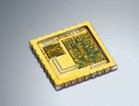
In IMS booth #3513 in Montreal, Canada this week, KCB, an AS-9100 certified designer and manufacturer of hi-rel SMT devices, is introducing some of their most recent semiconductor packaging techniques. One such technique, recently employed for a military customer in the AESA radar market, was a custom hermetic device that included two chips, a driver, on-board DPS, a DVA capability, and a PA stage. KCB designed a multi-layer HTCC hermetic package featuring unique heat dissipation while allowing access to phase shifter and attenuator controls via TTL. Using an innovative weightless gold/tin eutectic die attach method, KCB was able to mount each die simultaneously while ensuring and maintaining void-free attachment. This allowed KCB to meet the high volume demands of the phased array application while maintaining the quality of the device via void-free attachment.
For more information, visit www.KCBsolutions.com.
SOURCE: KCB
