
EM Simulation: Evolution Within Circuit Design
Dr. John M. Dunn, AWR
Electromagnetic (EM) simulation has become commonplace for RF and microwave circuit designers. This viewpoint article examines current trends with regard to how designers use EM tools inside of circuit simulators.
EM Simulation Evolves
Looking back to the early 1990s, there were essentially two popular EM simulation technologies available: the method of moments (MoM) for planar structures and the finite element method (FEM) for both 2D-cross sectional and 3D structures. These simulators typically focused on simple (compared to today’s designs) structures such as a via, a bend, or a waveguide.
Today, of course, the problems being simulated are much larger. Entire RF boards, chips, and modules can now be investigated with an EM simulator, ranging from MoM to FEM, as well as finite-difference time-domain (FTDT) and the finite integration technique (FIT). So what has happened to the 2D FEM-based cross-sectional EM solvers of the early years? They are still in use but have been hidden (so to speak) from the designer in what is now more commonly accepted as an “EM model.” For example, consider the transmission line that’s used in circuit simulation/schematics. The model behind the transmission line that is placed on the circuit schematic is actually the results of an EM simulation, while the designer is largely unaware that an EM simulation is being run behind the scenes.
Obviously, EM simulators can model much more complicated structures than 20+ years ago, because geometry complexity has increased with computational capability, as should be expected. In addition, the use of EM models, where EM simulation is used behind the scenes without the designer having to explicitly set up the simulation or even know it is occurring, is becoming widespread.
It has also become easier to create an EM model when one is not supplied by the vendor. EM simulators typically enable the designer to control the layout using parameters that can be swept, thereby creating an EM model with parameters controlling the various layout dimensions. Consider this trend: In the era of the 1990s, EM simulators were typically standalone tools. The designer had to redraw the stackup and layout, and manually import the results (typically S-parameters) back into the circuit simulator. In addition to the inconvenience and time drain, this approach was then and still is prone to human error. To combat this, the major circuit simulation vendors now offer EM simulators that are integrated into their circuit environments in a number of ways. Following are two examples.
Figure 1 below shows an example of the EM extraction flow.

Figure 1: MMIC and module in the circuit design software. The inductor on the MMIC is selected to be sent out to the EM planar simulator.
The circuit is a microwave monolithic integrated circuit (MMIC) mounted on top of a module. Bond wires connect the two structures. The designer can send various parts of the circuit out to the appropriate EM simulator or modeling tool. In the MMIC schematic, the inductor has been selected to be sent out to the planar simulator. When the designer asks for the amplifier’s response, the layout of the inductor is automatically sent to the EM simulator, ports are added, and the S-parameters that are generated are used in the schematic to give the results. The designer does not need to manually set up the EM simulation in any way. The figure also shows that the bond wires could be sent out to the software’s 3D FEM simulator. The lines on the module are sent to an automated circuit extraction program, which uses models for the various lines and vias rather than running EM.
3D simulators are popular because of the generality of geometries they can simulate. However, they have traditionally been standalone tools, not well integrated into circuit simulators, because the layout environment in the circuit simulator is predominantly planar, and 3D shapes are limited to drawing a 2D polygon and extruding it in the vertical direction. It is therefore impractical to draw common objects like SMA connectors and coils.
Figure 2 shows how circuit design software circumvents this limitation by giving the designer access to preconfigured 3D layout cells.
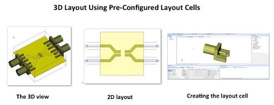
Figure 2: The layout uses pre-configured 3D layout cells for an SMA connector and an air coil. Layout cells can be created if they don’t exist using a 3D editor.
Here, the designer is using two 3D layout cells: an SMA connector and an air coil. There is no need to draw/redraw them — they are simply added to the 2D layout. The cells are controlled by parameters, so the various dimensions can be changed as appropriate. If the needed layout cell is not available, it can be created in a 3D editor that talks closely to the circuit software. Once drawn, the cell can then be used, and even added to the library if it proves useful. The designer can now run the FEM simulator, without ever having to leave the circuit environment.
Conclusion
A number of trends in EM simulators for circuit designers are going to develop over the foreseeable future, the most obvious of which is increasing numerical capacity for looking at more complicated geometries. This viewpoint article has quickly focused on more tightly integrating the EM simulator into the circuit simulation environment. EM models use an EM simulator, yet the designer is unaware of its existence. In a sense, EM is disappearing! Of course, the reality is that EM is becoming more pervasive in circuit design than ever, it is just becoming easier to use so that designers can focus on the real problem — getting a circuit designed and working correctly so the end product provides the best performance possible and can go to market more quickly and economically.