
Solid State Microelectronics, Microfabrication Enable mmWave TWT High-Power Amplifiers And Power Modules
By R. Jennifer Hwu And Larry P. Sadwick
Further development of microfabrication may enable not only wider bandwidth, but also higher frequency operation of high-power TWTs toward and into the terahertz range.
Future U.S. military superiority will be highly dependent on information dominance and advanced command, control, communications, computers, combat systems, intelligence, surveillance and reconnaissance (C5ISR) capabilities, which fall largely within the realm of satellite communications (SATCOM). The future of info-centric warfare will require electromagnetic access for collecting and distributing information; however, the electromagnetic spectrum, as the heart of current and future warfare, remains highly contested and congested.
To address this problem, transmitters supporting advanced space-based radio frequency (RF) communication systems must have millimeter wave (mmWave) high frequencies. At the same time, as with any SATCOM components, the mmWave frequencies will need to assure high power capability, wide to ultrawide bandwidth, high efficiency, and low cost. Furthermore, mmWave power devices and their associated systems exposed to radiation in space may experience power resets, safing (de-arming), performance degradation, and/or temporary or permanent failure, due to cumulative effects of long-term exposure or high energetic particle and/or photon fluence. Thus, these mmWave power devices must possess radiation-hard properties and be able to survive and operate through space radiation environments.
Current Limitations Of mmWave Power Tubes
Vacuum electronics technology, such as the traveling wave tube (TWT), is both old and new; its legacy is impressive and well-known, and its future looks even more promising. This is because there will always be applications — such as those associated with C5ISR, pushing further out in frequency, particularly into the mmWave range and beyond — and power-generation capabilities where solid state power devices fall off, leaving TWT power tubes to dominate the space. In addition, TWTs have demonstrated their ruggedness and insensitivity to radiation, making them the top choice for space-based operation due to reliable performance at high power, high efficiency, and relatively low cost.1,2
However, manual, cumbersome fabrication and manufacturing presents major challenges to higher frequency devices, where minute feature sizes and stringent dimensional accuracy are simultaneously required to ensure good reliability and performance.3,4 In addition, the conventional helix RF interaction circuit structure is no longer the circuit of choice, as it faces manufacturing, mechanical, and thermal limitations at mmWave frequencies.
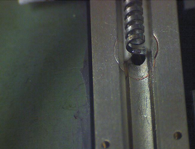
Figure 1. Two issues with helix circuits being pushed into the mmWave range: (1) The fragile helix needs to be supported by three rods — since it is cut open from the top, only two can be seen here — which also handle all thermal dissipation of the helix, and (2) a major wear-out mechanism is metal fatigue caused by thermal expansion and contraction of the connection (see this small connection through the hole in the picture) where the center connector of the RF output connector meets the helix structure.
Microfabrication And Integrated Microelectronic RF Interaction Circuits
For the past decade, new manufacturing techniques5-9 have been leveraged to address this issue, including solid state microfabrication for the manufacture of conventional helix and coupled cavity RF interaction slow wave structures (SWSs).
The manufacturing of high frequency components, such as the W-band helix structure, has been tried in some of these studies. However, the planar and layered nature of solid state microfabrication does not lend itself well to helix slow wave structure fabrication. As a result, for example, a helix structure with square cross section,6 although successfully produced, is not ideal for achieving high-efficiency operation of a conventional helix. Further, while coupled cavity structures for the W-band are easily microfabricated to precise specifications, manual assembly of a large number of these microfabricated coupled cavity structures can still render feature misalignment and accumulated pitch error, which is not acceptable at MMW frequencies.
To ensure the physical feasibility of microfabrication, and to best utilize its improved precision and integration advantages, the microfabrication techniques and integrated RF interaction circuit structures suitable for solid state microelectronics also have been applied to MMW TWT design and manufacturing. For example, various ways of microfabrication have been studied for folded waveguide (FWG) slow wave structures at different frequencies, especially high mmWave up into high sub-mmWave frequency.10-14 In addition, new integrated RF interaction circuit structures, such as grating type (for example, staggered single vane and double vane15-17) and ladder type,18-20 also have been developed and studied. All three types of slow wave structure mentioned here have been successfully microfabricated at sub-mmWave frequencies (100s of Ghz).
By employing these new integrated RF interaction circuit structures, suitable for microfabrication at mmWave frequencies, TWT slow wave structures can be produced with small features, high precision, and high yield batch process to support improved reliability, manufacturing yield, and the quality of MMW power tubes. For example, Fig. 2 shows the wafer scale fabrication of a mmWave (at Ka-band) RF interaction circuit structure. Note that more than 20 circuit structures can be built on a six-inch wafer at the same time. Fig. 3 shows a close-up view of the straight wall and smooth surface created for a W-band integrated RF interaction circuit through microfabrication.
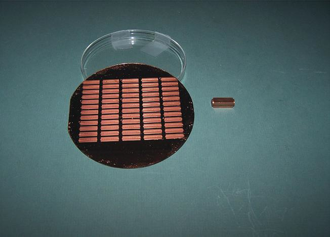
Figure 2. Borrowing from solid state microelectronics techniques, multiple RF interaction circuit structures microfabricated on a wafer
In addition to supporting the high frequency capability of the power vacuum tube, these integrated RF interaction circuit structures are either built on a platform or integrated with a waveguide — or both. Relatively higher power than conventional helix structure also can be achieved by employing advanced microelectronic technology in mmWave power tubes. Still, these microfabricated structures will not be able to compete with conventional helix TWTs in certain performance metrics, such as bandwidth. However, they do offer enough bandwidth for most current requirements and offer the potential to take the place of helix at mmWave and higher frequencies.
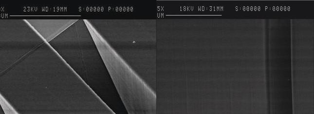
Figure 3. Zoom-in views of an RF interaction circuit for a mmWave power tube achieved through microfabrication
Note that high-power-at-high-frequency capabilities can be combined with the low-cost and high-yield production of solid state microfabrication to support the relatively higher volume demands in dual-use mmWave military and commercial satellite communications: mmWave TWTs from the Ka- to W-bands, with typical output powers of more than 100 Watts (and some up to 1 kW), have been reported based on this microelectronic approach.3,21,22 Microfabricated TWTs also have shown suitability for high-temperature and high-radiation operations.23,24
Power-Combining Technique Applied To SSPAs In Power Tubes To Achieve Very High Power
The quasi-optical power-combining technique that has been employed for decades to increase the output power level of solid state power amplifiers (SSPAs) also can be applied in mmWave TWTs to enable the continual increase of output power, even at very high frequencies. Specifically, an array of distributed RF interaction circuits is integrated and microfabricated together to achieve higher TWT output power.25- 27 Similar to the quasi-optical spatial power-combining solid state device array, this is accomplished by adding the symmetry boundary conditions between the two circuits.
With the symmetry boundary conditions, the performance of each circuit element is the same as that of the others, and the performance of the linear array is similar to that of the single device, except the total power of the linear array is the sum of individual devices in the array. As a result, the number of distributed RF interaction circuits is increased to increase the overall output power while keeping the same performance — including bandwidth, efficiency, etc. — possible from the individual device. This is done without the need to significantly increase the physical size and complexity of the power amplifier design, since multiple RF interaction circuits are integrated and fabricated as a whole unit into one vacuum envelope.
An important factor in realizing the power potential and performance flexibility of the mmWave high-power TWT is the manufacturability — or, specifically, the manufacturing accuracy — of the multiple RF circuit structures. Solid state microfabrication methods provide precision of the period along the length of the RF circuit structure, as well as align one unit RF circuit channel with the next (for example, within a ìm or less). This is especially true when higher power and, as a result, a large array is involved. Through this power-combining approach, power requirements from few kWs to hundreds of kWs can be achieved, depending on the frequency and size of the array (Fig. 4).
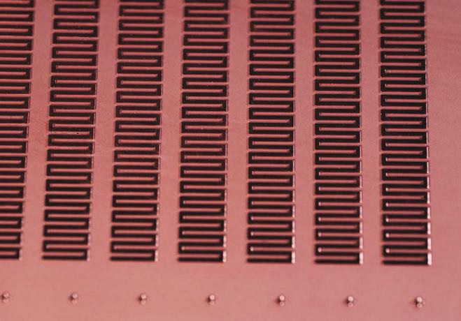
Figure 4. Quasi-optical power-combining array, with seven RF circuit channels, for a W-band high-power TWT
Reduced Parts Counts And Process Steps Increase Reliability
The use of batch, high-yield, and high-level-integration production processes associated with microfabrication techniques results in lower production costs and high reliability, with greatly reduced parts counts and component variations. For example, consider the parts and process step counts from a microfabricated 30-31 Ghz, 50 Watt TWT, versus a conventional helix TWT of similar performance parameters (Table 1). The TWT employing solid state microfabrication techniques has > 56 percent reduction in parts count, > 84 percent reduction in brazing joints, and > 50 percent reduction in alignment fixtures.3
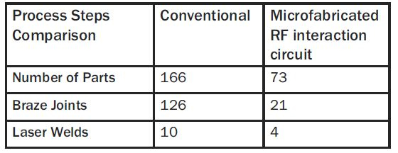
Table 1. Parts and process steps counts: conventional TWT versus Ka-band TWT employing solid state microelectronic and microfabrication techniques
To verify our expectation of a microfabricated TWT’s higher reliability, a theoretical study based on MIL-HDBK-217F, MILPRF- 1L, and the experience TWT failure rate model were used to calculate the mean time before failure (MTBF) of both the conventional TWT and the microfabricated TWT employing integrated RF interaction circuit structure. The side-by-side comparison shows more than a 10-fold reliability improvement (Table 2). Furthermore, mmWave TWTs can have even higher levels of integration in their construction (i.e., less parts and process steps counts) than this 2004 study achieved.3
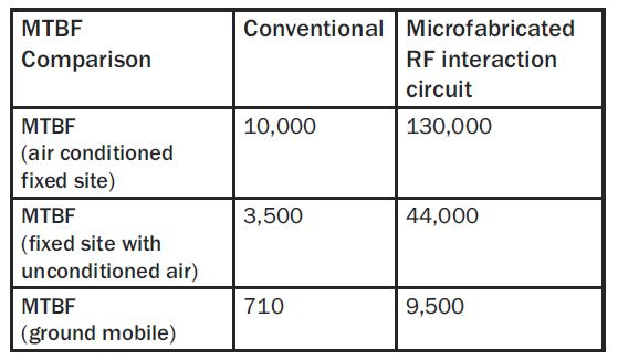
Table 2. Theoretical MTBF calculations: conventional TWT versus microfabricated Ka-band TWT (based on parts and process steps counts in Table 1)
Additive Manufacturing Can Further Reduce Manufacturing Complexity
Power tube making involves highly skilled processes and meticulous procedures. As a result, both in general and in surmounting scaling challenges to mmWave frequencies and above, the industry could benefit from advanced manufacturing’s improved precision and higher integration. For example, studies have been performed to apply more advanced circuits — specifically, additive 3D printing manufacturing technology — to the making of RF interaction circuits of MMW TWTs.28-29 One such example is a 3D-printed, W-Band folded waveguide RF interaction circuit (Fig. 5).28 Note that, although special surface processing must be conducted to reduce the surface roughness down to Ra between 20 to 50 nm, the 3D-printed W-Band RF interaction circuit successfully passed helium leak checking.28
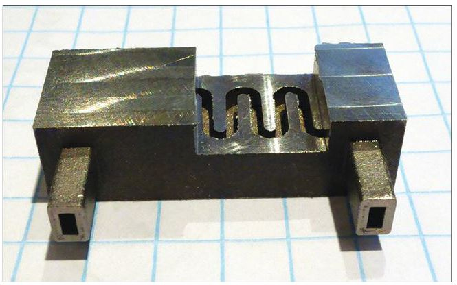
Figure 5. 3D-printed, integrated W-band RF circuit with input/output ports and tube body printed together with the actual folded waveguide RF interaction circuit
Fig. 6 shows the surface roughness of a W-band part before (A) and (B) after going through the material processes developed for the 3D-printed vacuum tube parts. Although it is difficult to 3D print copper at this time, to address electrical conductivity concerns, copper plating can be used on a 3D-printed circuit to achieve high conductivity.
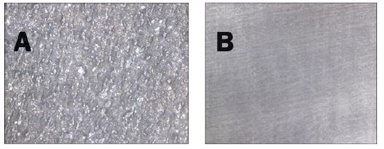
Figure 6. Surface roughness of 3D-printed part before (A, 1.6 μm) and after (B, 20 nm) post machining
Conclusion
Based on the capability to create fine features and a range of circuit sizes, microfabrication techniques have been demonstrated for use in high mmWave and sub-mmWave TWT circuit structures. While microfabrication may not replace conventional helix TWT at lower frequencies, in the microwave region, microfabrication remains useful so long as it remains difficult to reliably produce helix at high mmWave frequencies. As applications for mmWave power continue to develop, there exists a need to employ solid state microfabrication in TWT RF interaction circuit structure-making, including the development of RF interaction circuit structures suitable for microfabrication that are able to satisfy the bandwidth requirements of future systems. Additionally, new RF interaction structures suitable for higher-level integration — able to address increasing frequency, power, and thermal capacity of mmWave TWTs — will need to be further developed and studied.
Despite a number studies producing significant results in support of solid-state microfabrication to enable high-power vacuum devices operating in mmWave frequencies and above, additional work is needed to fully take advantage of these techniques. Further development may enable not only wider bandwidth, but also higher-frequency operation of high-power TWTs, toward and into the terahertz range.
Dr. Larry Sadwick is the CTO and cofounder of InnoSys, Inc. Dr. Sadwick received his doctoral degree in electrical engineering from UCLA. He has worked at the University of Utah as a tenured faculty member in the Department of Electrical and Computer Engineering, Unisys, Xerox, and TRW as a member of the technical staff. Dr. Sadwick has published and presented numerous papers and holds a large number of patents. He has served as the conference chair of the Terahertz Technology and Applications conference since 2010. Dr. Sadwick’s technical accomplishments have received recognition, including Utah Genius Award and Utah Innovation Award.
Dr. Jennifer Hwu is the president, CEO, and cofounder of InnoSys, Inc. She heads the RF design team of InnoSys. Dr. Hwu received her master of science and doctoral degrees from UCLA. She was a tenured faculty member of the Department of Electrical Engineering at the University of Utah and worked for TRW, Electronics and Technology Division as a member of the technical staff prior to that. She currently serves on the governing authority as the Utah governor’s appointee for the Utah Science Technology and Research (USTAR) initiative.
References
- Eric F. Nicol ; Bill J. Mangus ; John R. Grebliunas ; Kyle Woolrich ; and James R. Schirmer, “TWTA versus SSPA: A comparison update of the Boeing satellite fleet on-orbit reliability,” 2013 IEEE 14th International Vacuum Electronics Conference (IVEC), 21-23 May 2013.
- J.M. Weekley and B.J. Mangus “TWTA versus SSPA: a comparison of on-orbit reliability data,” IEEE Transactions on Electron Devices, Volume 52, Issue 5, pp 650 – 652, May 2005.
- L. P. Sadwick, R. J. Hwu, and D. B. Anderson, “Microfabricated Next-generation Millimeter-wave Power Amplifiers”, RF Design,/Defense Electronics, pp 11-23, February 2004.
- Microfabricated Traveling Wave Tubes for High Power Millimeter-Wave and Thz-regime Sources, http://www.dtic.mil/dtic/tr/fulltext/u2/a458532.pdf
- Helical waveguide millimeter wave TWT - IEEE Conference Publication http://ieeexplore.ieee.org/document/32834/
- Microfabricated 94 Ghz TWT - IEEE Conference Publication http://ieeexplore.ieee.org/document/6857547/
- Square helix TWT for Thz frequencies - IEEE Conference Publication https://ieeexplore.ieee.org/document/5612585/
- A Microfabricated Planar Helix Slow-Wave... (PDF Download Available) https://www.researchgate.net/publication/274013809_A_Microfabricated_Planar_Helix_Slow-Wave_Structure_to_Avoid_Dielectric_Charging_in_TWTs
- J.H. Booske, H. Jiang, C.L. Kory, R.L. Ives, S. Sengele, D.W. van der Weide, S. Limbach, P. Borchard, “Microfabrication technologies for millimeter-wave and terahertz regime vacuum electronic devices and components,” Tri-Service Vacuum Electron Device Workshop, 13-15 Sept, Albuquerque, NM (2005).
- S. Sengele, J. Welter, S.-J. Ho, H. Jiang, J.H. Booske, D.W. van der Weide, S. Limbach, C.L. Kory, M. E. Read, R.L. Ives, “Microfabricated Folded Waveguide TWT circuits and components for the Terahertz and Millimeter wave regimes,” 6t IEEE Intl. Vacuum Electronics Conference, Huis ter Duin, Noordwijk, Netherlands, 20-22 April, 2005.
- Design of a 300 Ghz Band TWT with a Folded Waveguide Fabricated by Microelectromechanical Systems https://link.springer.com/article/10.1007/s10762-016-0306-5
- Simulation and Microfabrication Development of Folded-Waveguide Slow-Wave Circuit for Thz Traveling-Wave Tubes https://www.duo.uio.no/bitstream/handle/10852/11076/dravhandling-zheng.pdf?sequence=3
- Folded waveguide traveling-wave tube sources for terahertz radiation, IEEE Transactions on Plasma Science https://scholar.google.com.tw/scholar?um=1&ie=UTF-8&lr&cites=8938258817335483969
- MEMS-microfabricated folded waveguide circuit for Thz TWT https://www.researchgate.net/publication/277680085_MEMS-microfabricated_folded_waveguide_circuit_for_THz_TWT
- High efficiency and high power staggered double vane TWT amplifier enhanced by velocitytaper design http://ww.jpier.org/PIERC/pierc66/05.16050305.pdf
- Experimental characterization of LIGA fabricated 0.22 Thz TWT circuits http://ieeexplore.ieee.org/document/5746982/
- Experimental, numerical and analytical studies of the staggered double vane structure for Thz application http://ieeexplore.ieee.org/document/5193375/
- A ladder circuit coupled-cavity TWT at 80-100 Ghz, 1986 International Electron Devices Meeting, http://ieeexplore.ieee.org/document/1486487/
- R. J. Hwu, Jishi Ren, Derrick K. Kress, and Larry P. Sadwick, “81-86 Ghz E-band 90 Watts High Power Traveling Wave Tubes”, 2016 IEEE IVEC. http://ieeexplore.ieee.org/document/7561862/
- L. P. Sadwick et al., “A new improved slow wave structure for broadband millimeter wave traveling wave tubes”, 2014 IEEE IVEC, pp. 313-314. http://ieeexplore.ieee.org/iel7/6847484/6857455/06857615.pdf
- L. P. Sadwick et al., “W-Band SSVDTM High Power Amplifier and Electronic Power Conditioner and Modulator and Supply, 2010 IEEE IVEC, pp. 503-504.https://www.researchgate.net/publication/241169655_205_W-band_SSVD_high_power_amplifier_and_electronic_power_conditioner_modulator_and_supply?ev=auth_pub
- Q-band 120 watts high power traveling wave tubes, 2017 18th IEEE International Vacuum Electronic Conference http://ieeexplore.ieee.org/document/8289543/
- L. P. Sadwick, Y. J. Zhang, D. J. Schaeffer, and R. J. Hwu, “Microminiature thermionic vacuum tube diodes,” 2013 International Electron Device Meeting (IEDM), 5-8 December, 2013.
- L. P. Sadwick, R. J. Hwu, and D. Kress, High Temperature UHF SSVDTM Power Amplifiers, 39th IEEE Aerospace Conference, Big Sky, Montana, 3-10 March, 2018.
- R. J. Hwu, J. Ren, D. K. Kress, and L. P. Sadwick, “Quasi-Optical Spatial Power Combining Traveling Wave Tubes”, 2014 15th IEEE IVEC, pp 103-104, 22-24 April, 2014.
- R. J. Hwu, Jishi Ren, Derrick K. Kress, and Larry P. Sadwick, “Ku band, 100 kW Traveling Wave Tube based on Large Quasi-Optical Spatial Power Combining Array”, 2016 17th IEEE IVEC, 19-21 April, 2016.
- R. J. Hwu, Jishi Ren, Derrick K. Kress, Jordan M. Krebs, and Larry P. Sadwick, “W-band Quasi- Optical Spatial Power Combining High Power Traveling Wave Tubes”, 2016 17th IEEE IVEC, 19-21 April, 2016.
- 3D printing additive manufacturing of W-band vacuum tube parts, 2016 17th International Vacuum Electronic Conference, http://ieeexplore.ieee.org/document/7561864/
- Measurements of structures for vacuum electronic sources manufactured by 3D printing https://ieeexplore.ieee.org/abstract/document/8289669/a