
Graphene Circuit Ready For Wireless

By Shu-Jen Han of IBM Research
Graphene, one of the world’s thinnest electronic nanomaterials, has long held the promise as a wonder material in everything from flexible touchscreens to super-fast circuits. It’s that interest in semiconductors that led my team to build the world’s most advanced, fully functional integrated circuit made of wafer-scale graphene – 10,000 times better performance than previously reported efforts.
Our demonstration has the potential to improve today’s wireless devices’ communication speed, and lead the way toward carbon-based electronics device and circuit applications beyond what is possible with today’s silicon chips. Integrating graphene radio frequency (RF) devices into today’s low-cost silicon technology could also be a way to enable pervasive wireless communications allowing such things as smart sensors and RFID tags to send data signals at significant distances.
What is Graphene?
Graphene is a single layer of carbon atoms packed in a honeycomb structure. Its electrical, optical, mechanical and thermal properties make it well-suited for wireless, or RF, communications.
Circuits built on graphene could allow mobile devices – tablets to wearables – to transmit data much faster, in a more cost-effective manner, than today’s silicon-based chips. For example, the circuits we built for wireless receivers consume less than 20 mW power to operate, while also demonstrating the highest conversion gain of any graphene RF circuits at multiple GHz frequency – successfully receiving and restoring a digital text message (“I-B-M”) carried on a 4.3 GHz signal without any distortion.
Fabrication of a true integrated circuit is challenging because it’s easy to damage a sheet of graphene during the fabrication flow of conventional integrated circuits. So, while we had shown it was possible to build an analog graphene integrated circuit with a broadband frequency mixer in a 2011 proof of concept, the graphene transistor performance was inevitably degraded due to the harsh fabrication processes.
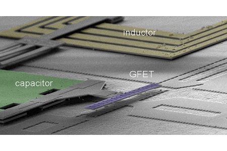
Tilted view scanning electron microscopic (SEM) image revealing the integration of key components in IC with enlarged view showing the advanced gate structure of the graphene field-effect transistors (GFET). Inset image shows crosssectional SEM of embedded T-shaped gate. Scale bar, 500 nm.
The team decided to flip their approach by completely reversing the conventional silicon integrated circuit fabrication flow, leaving graphene transistors as the last step of integrated circuit fabrication. This resulted in preserving graphene device performance. And it resulted in the first time that graphene devices and circuits could perform modern wireless communication functions comparable to silicon technology.
For more, read Nature Communications paper “Graphene Radio Frequency Receiver Integrated Circuit” by Shu-Jen Han, Alberto Valdes Garcia, Satoshi Oida, Keith A. Jenkins and Wilfried Haensch. The breakthrough is also a major milestone for the Graphene Open Manufacturing program, funded by DARPA.
Original Release: http://ibmresearchnews.blogspot.com/2014/01/graphene-circuit-ready-for-wireless.html#fbid=86Z4tmYzXlo
Source: IBM T.J. Watson Research Center