
Design Of A Cost-Effective, Hybrid Input-Matched GaN Transistor For S-Band Radar Applications
By Robert Smith & Liam Devlin, Plextek RFI; and Richard Martin & Thomas Landon, Qorvo Inc.

The use of gallium nitride on silicon carbide (GaN-on-SiC) technology in high-performance RF power amplifiers (PAs) is now widespread. While the cost per unit area of GaN is still higher than that of competing technologies, such as gallium arsenide (GaAs) or LDMOS, the technology has now matured to the point where the transistor cost per watt of RF output power is lower than that of GaAs.
Active phased-array radars can contain hundreds of amplifiers, so any cost reduction that can be achieved on a single amplifier quickly adds up to significant overall cost savings. At the same time, the RF performance of the system is paramount, and power amplifiers that use GaN-on-SiC transistors have achieved excellent power and efficiency.
This article describes the design of a hybrid input-matched GaN transistor, which includes internal input matching realized on a passive GaAs die. Unlike a pre-matched transistor, which is not fully matched to 50 Ω, the input of this transistor is internally matched to 50 Ω. This transistor is termed ‘hybrid’ due to its use of two separate semiconductor technologies. This approach provides the performance of GaN and the convenience of internal input matching at a reduced cost, compared to a GaN MMIC.
The transistor’s internal input matching is designed for the 2.7 – 3.5 GHz frequency range. For S-band radar applications, it is common to only use part of the frequency band. The output matching network can therefore be implemented on the PCB to allow large-signal performance to be optimized for output power or efficiency (or a compromise between the two) over the desired frequency band.
The transistor can be used as an output stage in an active phased-array radar system, or as a driver amplifier for a higher-power output stage. An accompanying PA reference design with an output matching network tuned for optimum efficiency between 2.7 to 3.1 GHz has also been developed, and is described below.
Transistor Implementation Strategy
There are several practical approaches for the realization of GaN power amplifiers; a comparison of these options is presented in Table 1.
|
GaN MMIC (Input & Output Matched to 50 Ω) |
Discrete GaN Transistor with External Matching |
Hybrid Input-matched GaN Transistor (Input Matched to 50 Ω) |
|
|
Cost |
Highest |
Lowest |
Medium |
|
RF Performance |
Best |
Good |
Better |
|
Tunable |
Not tunable |
Input and output tunable |
Output tunable |
|
PCB Area |
Smallest |
Largest |
Moderate |
|
Customer Design Effort |
None |
High |
Medium |
Table 1 — Comparison of GaN Matching Approaches
GaN MMICs, internally matched to 50 Ω at both input and output, have the potential to provide the best RF performance — particularly at higher operating frequencies — and require the least space on a PCB. However, GaN MMICs generally are the most expensive of these options, and cannot be optimized for different operating bands. An example of a fully 50 Ω matched single-stage GaN PA design operating at X-band is described in an earlier paper.
A PA implemented using a discrete packaged GaN transistor is often the lowest-cost option, although it also tends to be the largest size. Examples of the design and realization of a range of GaN PAs, using discrete unmatched transistors, also were described earlier. In addition to occupying the most PCB space, this approach requires the highest level of design effort by the customer.
The per-area cost of GaN-on-SiC is undeniably higher than GaAs, especially when compared to a passive GaAs process with relatively few fabrication steps. It therefore makes sense to consider the use of a low-cost passive GaAs process for the input-matching network, and a high-performance GaN process for the transistors. Such a composite input-matched transistor allows costs to be significantly reduced, even accounting for the more complicated assembly process of mounting and bonding two die in a single package, without sacrificing performance.
Design Of The Hybrid Input-Matched Transistor
The transistor module consists of a GaN power bar and GaAs input matching die in an SMT plastic package, as illustrated in Fig. 1. An existing, commercially-proven, Qorvo GaN power bar was selected to meet the output power requirements. A suitable existing SMT plastic package measuring 6 x 5 mm was chosen, which helped to reduce development timescales. Plextek RFI then designed the bespoke GaAs input matching die and bond-wire transitions to match the input of the transistor to 50 Ω at S-band.
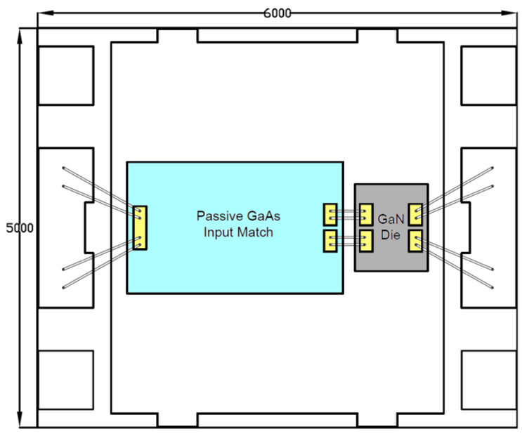
Fig. 1 — Internal layout of QPD1020 (dimensions in µm)
The passive GaAs die was designed to occupy the length of the package and so reduce the bondwire lengths. Similarly, the GaAs and GaN die were placed as close together as possible to minimize the bond wire length at this most critical point, where the impedance is at its lowest. As can be seen in Fig. 1, there is scope to reduce the size of the component through the use of an alternative custom package. While shortening the length of the GaAs input matching die would have been feasible, for the selected package this would have resulted in longer bondwire lengths, which would degrade RF performance.
The input matching network has a low-pass response implemented using series transmission lines and shunt capacitors. On-chip shunt resistors are also included on the passive matching die to improve in-band stability. This reduces available gain, and was therefore implemented with caution. Some additional modest off-chip stabilization may therefore be required to ensure unconditional stability down to very low temperatures. The GaAs input matching and bondwire interface to the GaN transistor were EM-simulated, and minor changes to the layout were made to compensate for the small changes in performance.
The GaN-on-SiC die was fabricated on Qorvo’s high-voltage 0.25 μm GaN process, which can be operated at drain bias voltages up to 50 V. The GaAs die was fabricated on a Qorvo passive process.
The resulting transistor can be operated in both pulsed and CW modes. Because of its CW capabilities, it can be used with long radar pulses. The gate biasing is implemented off-chip, which allows flexibility in the implementation of the low-frequency decoupling and allows for specific operating modes such as gate pulsing.
Measured Performance
The hybrid input-matched transistor was fabricated and the S-parameters of a number of samples were measured. Fig. 2 shows the measured S-parameters versus frequency of a typical part. The input match is greater than 15 dB between 2.8 GHz and 3.6 GHz, and the S21 is around 13 dB in-band. These measurements were made with no output matching network present, and with the transistor output terminated into 50 Ω. This means that the gain of amplifiers designed using this transistor will be higher than the S21 shown. The drain-source impedance of the transistor is largely capacitive at these frequencies, and therefore the unmatched output return loss appears highly reflective.

Fig. 2 — Measured S-Parameters of QPD1020 hybrid input-matched transistor only
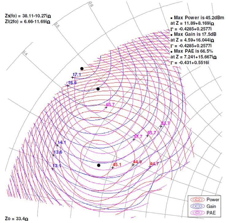
Fig. 3 — Load-Pull Measurements of QPD1020 hybrid input-matched transistor at 2.7 GHz
Fig. 3 shows load-pull measurements at 2.7 GHz (Z0 = 33.4 Ω) with the square marker positioned at the center of the efficiency contours. Figs. 4 and 5 show a similar set of measurements at 3.1 GHz and 3.5 GHz, respectively. A summary of load-pull results is presented in Table 2.
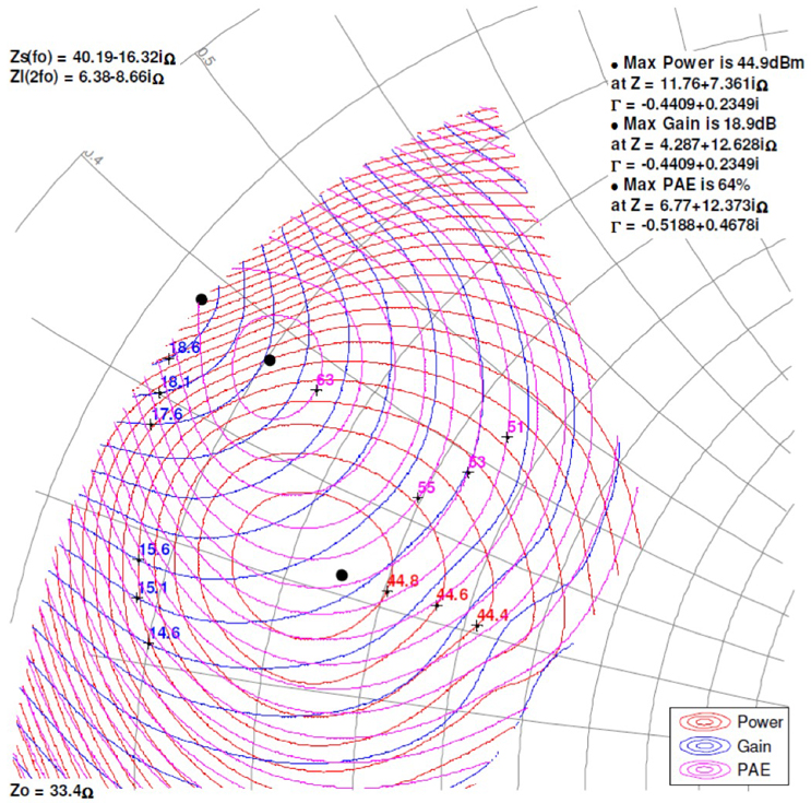
Figure 4: Load-Pull Measurements of QPD1020 hybrid input-matched transistor at 3.1 GHz
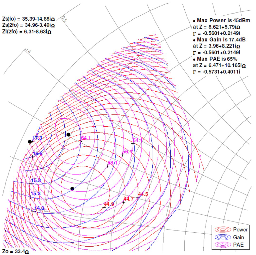
Figure 5: Load-Pull Measurements of QPD1020 hybrid input-matched transistor at 3.5 GHz
|
Frequency |
2.7 GHz |
3.1 GHz |
3.5 GHz |
|
POUT – Power Tuned |
45.2 dBm |
44.9 dBm |
45.0 dBm |
|
PAE – Power Tuned |
55.0% |
53.7% |
56.7% |
|
POUT – Efficiency Tuned |
43.6 dBm |
43.6 dBm |
43.9 dBm |
|
PAE – Efficiency Tuned |
66.5% |
64.0% |
65.0% |
Table 2 — Summary of Load-Pull Measurements of QPD1020 hybrid input-matched transistor
Power Amplifier Design and Implementation
The measured data presented above was used to design a 2.7 – 3.1 GHz power amplifier, which is provided as a reference design for the transistor. A circuit schematic of the PA is shown in Fig. 6.
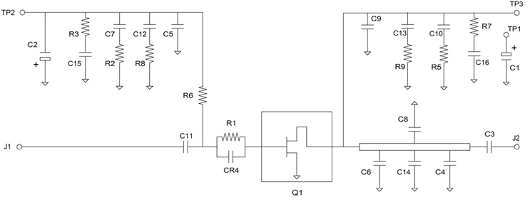
Fig. 6 — Schematic of the QPD1020 PA Reference Design
By implementing the output matching network on the PCB, the customer has flexibility in the operation of the PA. The PA can be tuned for greater output power or efficiency depending on the end application, and performance can be optimized for the required operating band. As an example of the trade-off between RF output power and efficiency, the load-pull measurements of the transistor module show that at 3.1 GHz a power match would result in 44.9 dBm (30.9 W) of output power at 53.7% PAE, whereas an efficiency match would result in 43.6 dBm (22.9 W) at 64% PAE (excluding output matching losses).
The output matching network of the reference design is a two-pole low-pass filter structure with an additional shunt capacitor to tune the second harmonic. Low-loss, physically small capacitors were used to reduce parasitic inductance and minimize losses. It is important to ensure that the capacitors on the output matching network can withstand the high DC operating voltage needed for the GaN transistor.
Due to the internal input matching network, very few input matching components are required on the PCB. A DC block, a pair of stabilizing resistors, and a series of gate decoupling capacitors are the only components required. It can be seen in Fig. 7 that most of the PCB at the input is occupied by a 50 Ω transmission line, and that the PCB can be made even smaller if the banana sockets included for ease of testing were not required.
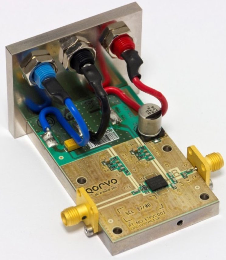
Fig. 7 — Photograph of the QPD1020 PA Reference Design
The PCB is constructed from Rogers 4350B laminate with a thickness of 20 mil (0.51 mm) and is bonded to an aluminum carrier. The PCB measures 40.1 x 63.0 mm (1.58” x 2.48”). The surface-mount plastic package results in simpler PCB assembly compared to traditional metal-ceramic packages. Copper-filled through-vias provide a low thermal resistance and low inductance path to the metal carrier. The temperature under the package can be measured through a hole drilled in the side of the aluminum carrier.
Power Amplifier Measured Performance
The measured S-parameters of a typical PA reference design are plotted in Fig. 8. It delivers 17.5 dB of small-signal gain at 2.7 GHz, and 17.9 dB at 3.1 GHz, with a slight positive gain slope. The input return loss is better than 10 dB across the band, reaching 30 dB at 3.15 GHz. The design was optimized for PAE rather than for high output return loss. It can be seen that the small-signal gain is greater than 15 dB between 2.4 GHz and 3.5 GHz, demonstrating the wideband nature of the internal input matching network. Five units were tested over the temperature range -40°C to +85°C with excellent repeatability observed between the units.
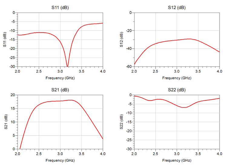
Fig. 8 — Measured S-parameters of QPD1020 reference design PA
The measured large signal performance of the PA across frequency and temperature is plotted in Fig. 9. The output power is a minimum of 21 W with 57% efficiency at P-3dB compression and 25°C, inclusive of all matching network and connector losses. The output matching network was tuned for optimum efficiency, and it can be seen that the efficiency is flat versus frequency.
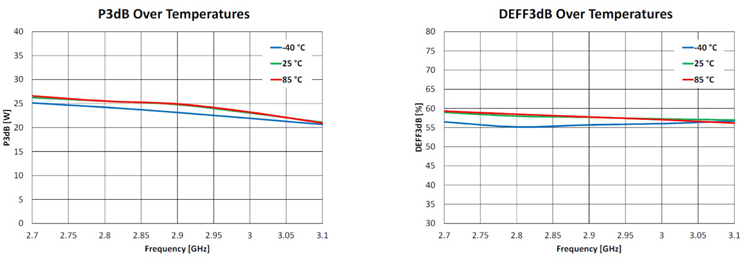
Fig. 9 — Output power (left) and efficiency (right) of QPD1020 reference design PA at P-3dB compression
Conclusions
The design of a GaN transistor with internal GaAs input matching (Qorvo QPD1020) has been described. The input matching network is designed for the 2.7 – 3.5 GHz frequency range, making the transistor suitable for S-band radar applications at a reduced cost compared to a GaN MMIC. The output matching network is implemented on the PCB to allow large-signal performance to be optimized for a desired frequency band. High performance is demonstrated using the transistor in a reference power amplifier designed between 2.7 to 3.1 GHz. The QPD1020 can be used as an output stage in an active phased-array radar system or as a driver amplifier for a higher power output stage.