
Logarithmic Amplifier/Detector Characterization Utilizing A Modern Vector Network Analyzer
By John Eckert, Agilent Technologies, Inc.
*Keysight Technologies Inc., formerly Agilent Technologies electronic measurement business
Logarithmic amplifiers (log amps) are commonly used in radar to compress wide-ranging signal amplitudes for subsequent digitizing and further processing. They are also used in radio frequency (RF) and microwave transmitters to control power and in receivers to indicate received signal strength. Two basic types of log amps exist. True log amps provide a logarithm of the actual input signal. Demodulating log amps or log detectors, on the other hand, provide a logarithm of the envelope of the input RF signal. Some log detectors also provide a limited or constant amplitude output that retains the phase information of the input signal.
When characterizing the log amp/detector, a number of RF measurements must be performed. At minimum, those tests include input (S11) match, output (S22) match, and output log conformance. Log detector errors include DC output bias and slope error. Limited outputs must also be measured for absolute power and input threshold. While these tests many appear straightforward, the conventional test systems typically used to perform them often face a number of limitations. Fortunately, many of these limitations can now be overcome with just a single instrument—a modern vector network analyzer (VNA). Let’s take a closer look.
Understanding Test System Limitations
The test systems used to characterize log amps/detectors are typically assembled from a variety of stand-alone instruments, including a signal generator, power amplifiers, a spectrum analyzer, power meters, digitizers, PC, custom software, and network analyzers. The stimulus for the device-under-test (DUT) is usually provided by a COT’s signal generator. When choosing a signal generator, the frequency and power range must cover the test needs of the DUT. The resolution and accuracy must also be met. Typical signal generators may specify the output power ranges from -130 to +5 dBm. If the DUT is to be tested from -50 to 0 dBm, for example, and the frequency falls in the range of the generator, one might assume that signal generator ‘Y’ is a good choice.
Signal generators use a combination of components to set the output power. They start by setting the output using a 0 to 100 dB, 10 dB per step, output attenuator as shown in Figure 1. This course resolution is enhanced by controlling the input power to the final output amplifier. To do this, the amplifier’s output is measured by a diode detector, or automatic level control (ALC) diode detector, that provides feedback to yield the requested power.
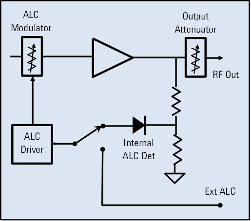
Figure 1: Shown here is a block diagram of an ALC diode detector.
The ALC diode detector must have enough bandwidth to cover the frequency range of the generator. The wide bandwidth of the detector raises its kTB noise (thermal noise floor), which reduces its sensitivity and limits the ALC range. Ranges are on the order of 30 to 40 dB for a microwave source. To change the output power greater than this amount, the output attenuator must be switched to a new value. Output attenuators consist of multiple cascaded stages. These stages are bypassed with mechanical switches to change attenuation values.
In this case, for low loss, wide bandwidth, accuracy, and high stability, mechanical attenuators are often favored over solid state attenuators. The downside, however, is that their internal switches wear out. Their lifetime is rated by the number of times they are actuated. Additionally, measurement accuracy can suffer, since changing the output attenuator changes the output impedance. This is most critical when switching to/from 0 dB when the DUT looks directly into the final amplifier.
Some signal generators have the ability to smoothly sweep the output power, which may be advantageous when testing log amps and detectors manually. However, the sweep is still limited to the ALC range. Keep in mind that the ALC diode detector is the limiting component in step-free power control. Modern VNA sources have more options with regards to ALC.
For DUTs that need to be tested beyond the ALC range, it is necessary to allow the output attenuator to switch. This should be carefully thought-out in an automated system.
Let’s say measurements are to be performed over a 50-dB power range at 100 different frequencies. Sweeping 50 dB and then changing frequency would yield 100 step attenuator changes per test. In contrast, sweeping one half of the power range at each frequency and then the other half of the range at each frequency results in 1 attenuator change per test.
If more power is needed to drive the DUT, an external power amplifier must be added between the source and DUT. This is problematic because there is no way of controlling the actual power into the DUT unless it is measured and continuously adjusted. A tuned receiver or spectrum analyzer can be employed to monitor the input signal. Power meters are another option, however, they are much slower and have less measurement range.
To measure the DUT detected output, a digitizer or digital voltmeter is needed. However, these instruments only provide an un-ratioed detector response. A best practice is to ratio the input and output measurements. The response must then be further processed to reveal the logarithmic conformance.
Finally, software is needed to synchronize the source stimulus, collect input/output data, and format the results. Both hardware and software maintenance over the life of the test system also have to be considered, along with development of a method for calibration and a test system uncertainty specification.
A Better Log Amp/Detector Test System
One simple way to minimize these limitations, while realizing several additional benefits, is to use a modern vector network analyzer. As an example, consider the graph in Figure 2, which shows the results of a log detector measurement.
With just a single setup, the results of swept frequency and swept power measurement are displayed on the VNA display. The upper panel of Figure 2 shows the swept power measurements. Trace 2 (TR2) is the limited output. It shows that the limiter’s output reaches its final power of 0 dBm at a -50 dBm input. Trace 1 is the swept input power. Trace 4 is the log detector output overlaid on input Trace 1.
With modern VNAs, you can add titles and give meaningful names to traces. A fourth trace, Trace 7 (Tr 7), is shown in the upper window and is the log error or log conformance trace. It is the difference between the input power and detected output. We normally think of the VNA measuring ratios of power at RF. Here we are using the ‘AI1’ input to create Trace 4. ‘AI1’ is one of two analog inputs on the rear panel that can be utilized as a measurement receiver and displayed as a trace. Trace 7, the log conformance trace, utilizes the VNA’s trace math feature to convert the log detected output to linear power terms that are subtracted from the input power trace. Markers indicate that the peak to peak log error is 1.29 dB over the DUT’s specified range.
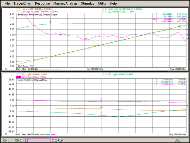
Figure 2: This graph displays swept frequency and swept power DUT measurement results.
The lower window of Figure 2 shows the swept frequency measurements log S11, log S22, and the transmission group delay S21 at the limiters output port. This is referred to as a two-channel measurement where one channel sweeps the power and the other frequency. Notice that the swept power ranges from -65 to +8 dBm — a 73-dB power range — and this is without the output step attenuator switching. Instead of using the internal source diode detector for ALC leveling, the VNA has the option to use one of its internal 100-dB range receivers for the ALC feedback. A power range of 73 dB is about the maximum at this frequency and will be more or less at other frequencies. The key point here is that the ALC range is no longer limited by the power detection.
VNAs have always had sophisticated calibration routines for removing errors associated with system imperfections. Variations in power are ratioed out, while error equations and known standards remove impedance and loss errors. Even absolute power (dBm) measurements are now possible. The calibration is performed in two steps. A traceable power sensor is connected to the VNA test set, and the VNA corrects the source power. Next, it uses the corrected source power to correct its own receivers. Then a standard S-parameter calibration corrects everything to the ends of the cables. This not only means that S-parameters are corrected at the DUT, but source power and absolute power measurements are as well.
Another key benefit of using a modern VNA is that their configurable test sets expose internal RF signal paths engineers can use to adapt the hardware for unique applications. A DUT that requires more power than the VNA is able to supply is easily addressed with one of these test sets. If an amplifier is simply connected between the cable and the DUT, it becomes part of the measurement results and not part of the test system. By removing a short jumper on the test set, an amplifier can be inserted between the internal source and coupled to a reference receiver. The physics of the amplifier are then encapsulated into the VNA and its fully calibrated measurements result.
Pre-production testing is a key area where the modern VNA shines. A great deal of testing takes place leading up to production, as this is when the bugs are worked out. No one likes to be ‘surprised’ at the production stage. The more data you collect early-on reduces your risk. Once a comfort level is reached, redundant data can be weeded out and the number of test points reduced. A complete picture is useful to understanding your DUT. A modern VNA provides an easy, cost-effective means of attaining this compete picture.
In this case, for example, the moden VNA used for testing has a ‘Quick Start’ measurement setup feature. To make measurements, the ‘Power Sweep’ setup was first selected. Then, the power and frequency parameters were entered. In mere seconds, swept power S-parameter measurements were being made. Next, the detector output was connected to the analog input and a trace was created. Finally, ALC was looked up in the VNA’s ‘Help’ file, and it was set to use receiver ‘R1’ for wide range power sweeps. Little more than an hour or so was spent getting the trace math correct.
Figure 3 shows a 3D plot of the detector output versus input power and frequency. A perfect device would yield a plane. Here, we see a gradual curve at the lower powers and saturation on the high end. Note that the device was purposely tested beyond its power and frequency specifications to provide a good view into the overall operation of the DUT.
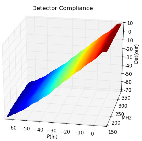
Figure 3: This 3D graph plots detector output versus input power and frequency.
In Figure 4 we see a much more detailed picture of how the DUT deviates from an ideal device. In Figure 2, Trace 7 provides just a single slice of this plot at 350 MHz. From Figure 4 one can very clearly determine that at the lowest power levels the error is due to low signal-to-noise ratio. At the highest power, the DUT is saturated and its response rolls off with frequency. Remember that the overall log response is created in piecewise steps. The piecewise segments errors appear as rolling hills. These 3D plots were generated by a thirty line program written in the open source Python programming language. Although, beyond the scope of this discussion, modern vector network analyzers can provide additional measurements under pulsed conditions.
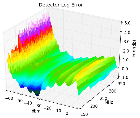
Figure 4: Shown here is a detailed comparison of the DUT to the ideal device.
Conclusion
While logarithmic amplifiers are widely used, characterizing them using a test system not plagued by a slew of limitations can be challenging. In fact, building a conventional log amp/detector tester from individual instruments, writing code, and doing acceptance testing could easily take months. Luckily, today’s modern VNA offers engineers an alternate solution — one that saves considerable time and effort.
About the Author
John Eckert is an RF/MW applications engineer and consultant with Keysight Technolgies. He has worked at Keysght/Agilent since 1987. John holds a BSEE degree from Oakland University, Rochester, Michigan.