
AlGaAs PIN Diode MMICs – Frequency & Power Capability
By Timothy Boles, MACOM
AlGaAs/GaAs PIN diode technology achieves loss, isolation, power handling and operational frequency capability that are unobtainable by alternative technologies.
By Timothy Boles, MACOM
Monolithic microwave integrated circuits (MMICs) based on high-power PIN diodes are increasingly used for many transmit/receive systems in advanced defense electronics and telecommunications applications. Examples of such systems include commercial and military SATCOM, civil and defense radars, half-duplex data links, Internet-protocol (IP)-based wireless LANs, and millimeter-wave (mmWave) imagers.
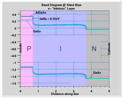
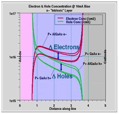
Fig. 1 — Band Diagram for Heterojunction PIN Diode & “I” Region Charge Confinement
For such applications, switches are required to have microwave and mmW frequency capability, as well as the ability to handle high power levels, low insertion loss, good matching, and fast switching — and, for non-reflective switches, good return loss in “off” state. This power handling requirement becomes especially challenging as the various systems’ frequency of operation moves from microwave to mmWave bands.
This application of bandgap engineering principles (Fig. 1) was used to create a structure using two dissimilar semiconductor materials, which have different Fermi levels, to produce a device that has a wider bandgap in the P+ anode region compared to the adjacent Intrinsic region (I region). This difference in bandgap enables a barrier height to be generated, which both enhances forward injection of holes from the P+ anode into the I-region, and retards the back injection of electrons from the I‑region into the P+ anode. This results in a P‑I‑N structure that has a significantly higher concentration of charge carriers reducing the RF resistance in the I-region of the heterojunction PIN device.
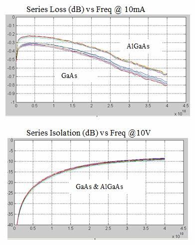
The off state capacitance of the diode will remain unchanged, since the thickness and resistivity of the I-region are unchanged. Measurements of fabricated diodes verified the simulation results, and demonstrated a 37 percent reduction of RF resistance in an appropriately formed AlGaAs/GaAs PIN diode, compared to a similar homojunction GaAs PIN diode under forward bias. The RF capacitance of the same two diodes under reverse bias was identical, as expected. These measured results for a series configured discrete PIN diode are shown in Fig. 2.
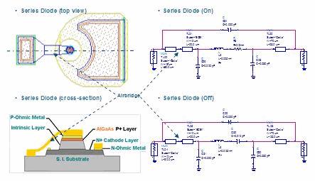
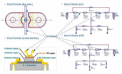
Utilizing three-dimensional EM software and a device structure simulator, models of AlGaAs heterojunction series and shunt configured PIN diodes were built up (Fig. 3 and Fig. 4). This modeling effort resulted in a simple off-state/capacitor and on-state/resistor model for the heterojunction PIN diode device.

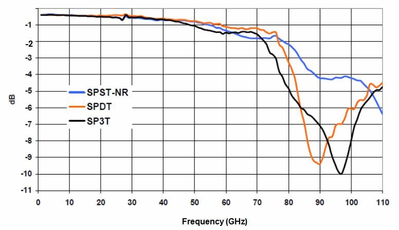
Employing classic textbook CT/Rs derived equations for high-frequency switches (above), a number of broadband switches — from RF through microwave and the high mmWave frequencies — were able to be realized in various series and series/shunt topologies, ranging from SPST through SP8T configurations. Representative high-frequency performance of this series of switches can be seen in the data of non-reflective SPST, SPDT, and SP3T series/shunt configured switches (Fig. 5). It can be seen that these switches are capable of achieving low insertion loss from 1.0 MHz to almost 80 GHz, which is over 16 octaves of instantaneous bandwidth.
While this heterojunction PIN diode switch capability has been well-received within the microwave community and has been applied to many military missile seeker programs, the thermal constraints of the series element has limited the incident power handling capability to a range of about 250 milliwatts through slightly-higher-than-one-watt of RF energy, depending on the frequency of operation. In addition, it can be seen that the upper frequency of operation is limited to approximately 75 GHz (Fig. 5). This drawback is a direct function of the resonance created by the diode capacitance, and the inductance associated with the series element airbridge.
Over the last decade, new system demands — primarily in military and commercial SATCOM — have required significant increases in the power handling at both microwave and mmW frequencies for switch, limiter, attenuator, and multi-function applications. This need for higher power handling, especially at mmW frequencies, led to a reconsideration of switch topologies and a further optimization of the basic AlGaAs/GaAs PIN diode structure.
For series configured switches, the RF energy in the “on” arm is flowing through the series PIN diode. It can be seen from the above equations that the RF power handling is limited by the dissipation and the insertion loss in this series element. For shunt configured switches, the RF energy in the “on” arm is not flowing through the PIN diode, but instead is being transferred from input to output through low-loss, high-Q transmission lines. In this case, the RF dissipation is due primarily to I2R losses in the metallic conductors, with the diode blocking element being DC reverse biased in an off-state. The insertion loss in this shunt configuration is limited by the diode shunt capacitance, and for multi-throw configurations, the loss in the λ/4 wave transformers needs to provide isolation between switch arms.
This analysis leads to the conclusion that, for higher power handling, the series element must be eliminated and an all-shunt switch architecture must be employed. This decision imposes a number of constraints and requirements on both the overall RF performance and the individual switch design components.
First, the isolation of an all-shunt design is entirely dependent on λ/4 wave transformers in each arm of the switch. The design of these transformers will limit the bandwidth to approximately 2:1, immediately implying that there is a tradeoff between operational frequency and bandwidth versus power handling. Second, the high frequency Q of these λ/4 wave transformers will ultimately determine the insertion loss of the switch. Lastly, the design of the active AlGaAs/GaAs switch element must be further optimized to include reverse bias breakdown, thermal resistance, capacitance, and parasitic contributions.
As discussed previously, software for electromagnetic and structure modeling is used to extract a resistance versus frequency curve for the forward-biased diode state and shunt capacitance versus frequency for the reverse biased diode mode, with special care being taken in consideration of the PIN diode mesa structure’s three-dimensional nature and the associated airbridged interconnections. In addition, this extraction needs to include all the intrinsic parasitic elements within the diode structure, incorporating bond pad capacitances, interconnection conductors, inductance and resistance, and the inductance of all ground vias.
Classic textbook theory predicts that the peak RF swing across a series element will produce a peak DC component and a resulting peak-to-peak DC swing (Equation 7 and Eq. 8):
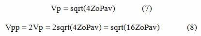
Further, the above correspondence between the limitations imposed on RF incident power handling by the resultant DC changes to the device bias condition can be summarized in Eq. 9. This equation establishes the minimum reverse bias required for a PIN diode in a high-power switch as a function of maximum CW, incident power, first reported by R. Caverly and G. Hiller.

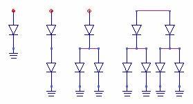
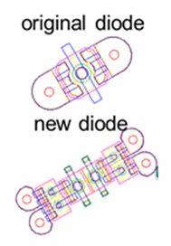
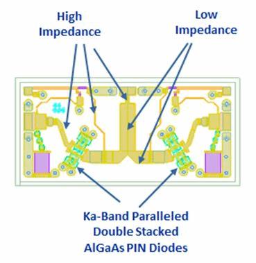
All previous shunt switches integrated a single shunt diode as the switching element in each arm, together with ¼ wavelength high- and low-impedance transmission lines and bias and termination circuits, all optimized for proper 50 Ω matching. To increase the power-handling capability of the fundamental AlGaAs/GaAs PIN diode design requires an increase of reverse bias voltage, which would normally imply an increase in the “I” region thickness and a reduction in the thermal resistance. Since there is a practical limit to increasing the “I” region thickness, a novel approach had to be taken to effectively double the “I” region thickness without changing the physical constraints of the process. In addition, higher incident power implies that the thermal resistance of the diode be reduced.
The next step is to merge this optimized 3D diode model with RF transmission lines and matching structures to complete the design of the monolithic switch as an integrated component. Using 3D EM software, the insertion loss, isolation, and terminal return losses of the final switch realization can be optimized, including the requisite interconnection bond wires. These 3D EM capabilities enable proper selection of matching elements to achieve low ripple Chebyshev response. This enables the insertion loss of the shunt diode switch to be reduced, which can be achieved by lowering the overall system impedance. The quarter wavelength bias network of each arm can be simulated to improve the impedance match at the desired frequency of operation. It was found that in order to maintain relatively high return loss and low VSWR, the common arm was also designed as a quarter wavelength section with less than a 50 Ω impedance. To compensate this reduced input impedance of the input, a section of high impedance transmission line connecting the quarter wavelength section with the input test pad is required.
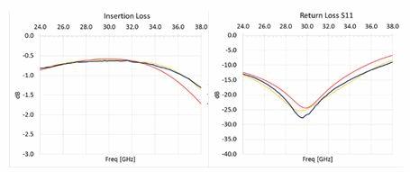
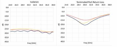
S-Parameter measurements were performed on the Ka-Band SP2T switch, and these are compared with simulation in Figs. 9 and 10. Measured data is shown in black, and EM simulation ranges based on process variation are shown in red and yellow, demonstrating excellent agreement.
Initial RF power testing results are shown in Fig. 11. The 40 watt SPDT shunt switch shown in Fig. 8 was measured in a narrowband fixture at 27.5 GHz at baseplate temperatures of 25°C, 60°C, 80°C, and 90°C. A 60 volt back bias was applied to the doubled stacked shunt diodes in the “on” arm at 7.5 volts, which results in a total current draw through the doubled stacked shunt diodes of 30 milliamperes of forward bias in the “off” arm. As can be seen in Fig. 11, the incident power to the switch was varied over a range of Pincident = +33.0 dBm (2.0 watts) to +46.1 dBm (40.7 watts). It can also be seen in Fig. 11 that high level insertion loss was approximately 1.2 dB over the range of incident power. This performance was observed on four switches and no failures were encountered at 46.1 dBm (40.7 w) power handling level through the entire baseplate temperature range of 25°C through and including 90°C.
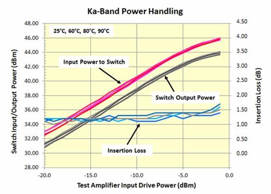
The 40 watt Ka-band AlGaAs/GaAs PIN diode shunt configured switch described above has demonstrated excellent small signal RF characteristics. This reflective switch has an insertion loss of <1.5 dB and an isolation of >27 dB over the 24 GHz to 38 GHz frequency range and is in excellent agreement with simulated results. Narrowband RF power testing at 27.5 GHz has been completed, and has resulted in the ability to handle 46.1 dBm, 40.7 watts of high frequency energy at a baseplate temperature of 90°C. It can be seen that AlGaAs/GaAs PIN diode technology sets new benchmarks for loss, isolation, power handling and operational frequency capability that are unobtainable by alternative technologies.
About The Author
 Mr. Boles holds a BA degree from St. Mary’s University and a MA degree from Washington University. Both degrees are in physics. He is the holder of 14 US patents and has authored/co-authored over 120 publications. Mr. Boles has been actively involved in the design, development, and manufacture of microwave devices and circuits for over three decades. Mr. Boles joined MACOM in 1991 and is one of nine current Technology Fellows at MACOM Technology Solutions. He also serves as the Chairman of the Technology Fellows Committee. His current assignment is as individual contributor in Technology Development.
References
- D. Hoag, J. Brogle, T. Boles, D. Curcio, and D. Russell, “Heterojunction PIN diode switch,” in 2003 IEEE MTT-S International Microwave Symposium Digest, 2003, vol. 1, pp. 255-258.
- D. Hoag, T. Boles, and J. Brogle, “Heterojunction P-I-N diode and method of making the same,” U.S. Patent 6 794 734, Sept. 21, 2004.
- D. Hoag, T. Boles, and J. Brogle, “Method of making heterojunction P-I-N diode,” U.S. Patent 7 049 181, May 23, 2006.
- “AG312 application note,” MA-COM, Lowell, MA, USA.
- T. Boles, J. Brogle, D. Hoag, D. Curcio, “AlGaAs PIN Diode Multi-Octave, mmW Switches”, COMCAS 2011, November, 2011
- S. M. Sze and K. N. Kwok, Physics of Semiconductor Devices, 3rd ed., Hoboken, NJ: Wiley, 2006.